 14 DAY TRIAL //
 As the amount of data transmitted over networks continues to grow, researchers have been looking for ways to make the use of optical signals more practical.
Optical networking offers the potential to dramatically improve data transfer rates by speeding the flow of data using light pulses, instead of sending electrons over wires.
The ability to use these signals could offer previously unheard of amounts of bandwidth and enhanced signal fidelity compared to current electrical data links.
For the 2007 Optical Fiber Conference, IBM scientists will reveal a prototype optical transceiver capable of reaching very impressive speeds, whose research was partially funded by Defense Advanced Research Project Agency through the Chip to Chip Optical Interconnect (C2OI) program.
"The explosion in the amount of data being transferred, when downloading movies, TV shows, music or photos, is creating demand for greater bandwidth and higher speeds in connectivity," said Dr. T.C. Chen, vice president, Science & Technology, IBM Research. "Greater use of optical communications is needed to address this issue. We believe our optical transceiver technology may provide the answer."
The breakthrough could transform the way data is accessed, shared and used across the Web for corporate and consumer networks, as the transceiver is fast enough to reduce the download time for a typical high definition feature-length film to a single second, compared to 30 minutes or more.
We're talking about information moving at speeds of 160 Gigabits - 160 billion bits of information per second - in what could be the next step in communications, computing and entertainment.
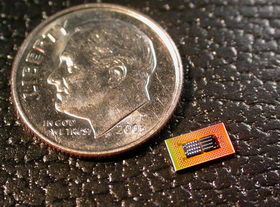
In order to achieve this new level of integration in the chipset, IBM researchers built an optical transceiver with driver and receiver integrated circuits in current CMOS technology, the same standard, high-volume, low-cost technology used for most chips today.
They then coupled it with other necessary optical components made in more exotic materials, such as indium phosphide (InP) and gallium arsenide (GaAs), into one, integrated package only 3.25 by 5.25 millimeters in size.
Optical connectivity could become viable for widespread use by shrinking and integrating the components into one package, and building them with standard low-cost, high-volume chip manufacturing techniques.
In a world of information, the continuous need for speed can only be beneficial for private consumers, in the end, because economic reasons will eventually render this new technology accessible to almost every businessperson and gamer alike, when these new optical chips will come with a "Made in China" label.