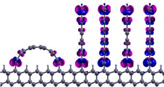
Rice University investigators – known for their leading role in studying graphene – propose a new use for the 2D, single-atom-thick carbon compound, this time as a free-standing wall placed on future generations of electronic devices.
Graphene wall arrays could be fashioned into ultrahigh density components of electronic or spintronic devices, says the team, which also included experts from the Hong Kong Polytechnic University.
If we are to take current microchip sizes as indicators, it could be argued that as many as 100 trillion bits graphene could fit on this surface. This is likely to happen in practice as well, since the international collaboration also discovered a way of affixing the carbon compound to the substrate.
Details of the newly-proposed use for graphene were published in a recent online issue of the esteemed Journal of the American Chemical Society (JACS). Rice theoretical physicist Boris Yakobson and HKP assistant professor Feng Ding were the leaders of the joint team.
The first substrates demonstrated to be capable of affixing graphene bits were made of diamonds, but the research team soon realized that soaring costs would prevent the technology from being employed at a large scale. As soon as possible, they also demonstrated the capability on nickel substrates.
Both diamond and nickel have the ability to bind the edge of graphene nanoribbon via chemical interactions. What the researchers were also looking for – a factor that eliminated other potential substrates – was maintaining graphene's inherent electrical or magnetic properties.
It's these traits that made the bi-dimensional carbon compound so attractive for the next generation of electronic devices in the first place, so ruining them would have served no purpose.
According to calculations compiled by Yakobson and Ding, the theoretical limit for the number of graphene wall field-effect transistors (FET) that can be placed on a square-centimeter chip is 100 trillion. This number literally blows in the face of limits imposed by Moore's Law.
“Moore liked to talk about silicon wafers in terms of real estate. Following his metaphor, an upright architecture would increase the density of circuits on a chip – like going from ranch-style houses in Texas to skyscraper condos in Hong Kong,” Yakobson explains.
He holds an appoint as the Karl F. Hasselmann Chair in Engineering at Rice, and is also a professor of materials science and mechanical engineering and of chemistry at the university. “This kind of strategy may help sustain Moore's Law for an extra decade,” he concludes.

 14 DAY TRIAL //