NAND Flash memory chips are kind of reaching their limit, capacity- and speed-wise, and advancing the manufacturing technology isn't helping as much as on the CPU front. So companies, in this case Toshiba, are putting new ideas into practice.
To overcome the limitations of single dies without having to take up more PCB (printed circuit board) space, Toshiba is creating 3D NAND chips.
Technically, Toshiba created and finalized the technology a while ago. It's just that mass production wasn't in progress until now.
In fact, mass production has still not begun, not exactly. Toshiba is finally transitioning to 3D NAND though, starting with its Yokkaichi Operations Center.
There, the second fabrication facility (Fab 2 for short) will be demolished. Brought down. Wrecked. Turned to rubble.
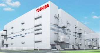
On the site, Toshiba will build a 3D manufacturing facility, and will even turn it into a joint venture co-founded and managed with SanDisk Corporation.
Demolition will start in May, and the new fab should be completed by May 2015. After that will come the hiring of personnel. So operations may not begin until the start of 2016.
By the end of it all, the new factory should be a wonder of manufacturing equipment for lithography, deposition and etching through joint ventures.
It's a real shame that Toshiba and SanDisk will have to contend with an already established supplier of 3D NAND memory.
You see, Samsung already has a factory open for 3D Vertical NAND Memory, and will keep itself busy shipping order and getting contracts signed between now and 2016.
It remains to be seen if the extra time taken by Toshiba and SanDisk yields 3D NAND chips that are in one way or another more advanced than Samsung's.
Probably not, because these things tend to come out at a similar level, quite possibly by design. Competition is the mother of innovation and whatnot.
Anyway, the new Toshiba-SanDisk fab will use LED lighting throughout the building and the latest energy-saving manufacturing equipment. It might even give them an edge over Samsung in the environment friendliness department. All in all, the facility should cut CO2 emissions by 15% compared to Fab 5 (the most advanced on the Yokkaichi site right now).
Sadly, the two partners haven't provided any hints as to what capacities and performance we can expect from their 3D NAND Flash memory. Nor did they say how their endurance compares to SLC (single-level cell) and MLC (dual/multi-level cell) chips.

 14 DAY TRIAL //