As some of you might know, Toshiba is one of the first companies that worked on the development of NAND flash memory, actually claiming that it invented it back in 1986. Although it's not quite sure that they were actually the first (the beginnings of NAND flash are still shrouded in mystery, as many companies worked in parallel on this very innovative concept), the fact of the matter is that they've continued their research and announced at the VLSI Symposium in Japan the development of a new NAND structure, dubbed SONOS (silicon oxide nitride oxide silicon), which will take the world of flash memory by storm.
According to Toshiba, the new structure is capable of increasing the cell density and data capacity without requiring a complete overhaul of the NAND manufacturing process. Moreover, the size of the flash memory chips that use the new SONOS structure won't increase dramatically, which means that the manufacturers of various NAND-based devices (including USB Flash Drives) won't have to significantly alter their products' design.
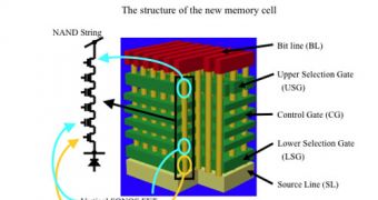
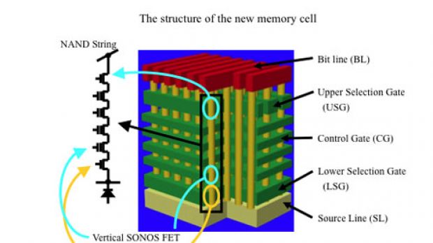
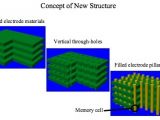
As the company informs us (via Fabtech), in the new technology, pillars of stacked memory elements pass vertically through multi-stacked layers of electrode material and utilize shared peripheral circuits. The key element in the manufacturing process is the "boring" of holes down through multi-layers of gate electrodes and insulator films. Pillars of silicon lightly doped with impurities are deposited to fill in the holes. The gate electrode wraps around the silicon pillar at even intervals, and a pre-formed nitride film for data-retention, set in each joint, functions as a NAND cell.
As mentioned earlier, Toshiba claims that this new array increases density without increasing chip dimension, as the number of connected elements increases in direct proportion to stack height. A practical example: a 32-layer stack provides 10 times the integration of a standard chip manufactured using current technology.
Quite obviously, research on the SONOS structure is far from over, and it will be a while before Toshiba comes up with a fully-functional model. However, if it does work as touted, this technology could alter the technological market as we know it, and deliver a final blow to all the forms of optical media.
We are just a few, but there are many of you, Softpedia users, out there. That's why we thought it would be a good idea to create an email address for you to help us a little in finding gadgets we missed. Interesting links are bound to be posted with recognition going mainly to those who submit. The address is  .
.

 14 DAY TRIAL //
