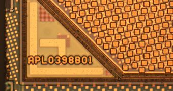
Following the teardown of the actual Apple iPad, people trained to go deep into the heard of chips and analyze them took on the task of popping open the A4 chip powering the Apple tablet. Chipworks has worked close with iFixit to bring folks a peek inside the iPad's chips, as well as a lesson on how semiconductor teardowns are conducted.
“Only one to two times per year does a device so much capture the minds of the market that it warrants braving planes, trains, automobiles, sleet, snow, and dead of night to get our hands on it,” Chipworks, the company whose business is semiconductor reverse engineering, says. “While Apple fans can't wait to use the latest device, we can't wait to . . . well . . . destroy it,” it reveals. “We braved the lines at a ‘local’ mall, got there early enough to be 20th in the pre-order line, only to bring the device home to our teardown lab.”
“Notably, we have been collaborating with our good friends over at iFixit who have published a detailed iPad teardown in a step-by-step format,” Chipworks further notes. Softpedia included details from iFixit’s findings in a Sunday report, which included various details on the Apple tablet and its successful debut.
iFixit shows the picture of a silicon wafer explaining that the visible squares each represent a chip, called a die. The processor die in the A4 is 7.3 mm on each side, for a 53 square mm total area, according to the renowned repair shop. A yield is the percent of working dies that you can get from a wafer as the one shown in the respective picture. The A4 is a Package on Package (PoP) chip featuring three silicon dies.
“Chipworks' unique angle in tearing down the iPad is to provide images down to the bare die,” the chip-teardown experts continue to stress. “[…] The Apple A4 processor is packaged just like the Apple iPhone processors using package-on-package technology. One for the microprocessor and one for the two DRAM die,” the company has deducted by grinding down layer after layer on the A4 chip. Readers can get the full scoop on this story here (from iFixit) and here (from Chipworks’ site).

 14 DAY TRIAL //