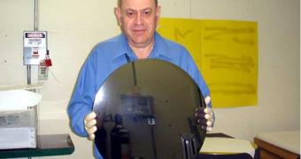
There have been a lot of discussions going on lately about the transition to 450mm wafers in the foundry industry, but TSMC seems set to do a lot more than just talk as the company plans to introduce its first 450mm production line in 2013, 2014 while its first such fab is expected to go live in 2015 or 2016.
The introduction of the new 450mm production line will occur at the same time as the company's introduction of the 20nm fabrication node and TSMC thinks that the new wafer size will allow it to reduce production costs and stay one step ahead of its rivals.
In fact, 450mm wafers can fit approximately 1.8 times more chips than their current 300mm counterparts and also require “fewer engineers’’ over time, said Shang-Yi Chiang, senior vice president of R&D at TSMC in an EETimes interview.
Chiang believes that attracting “good engineers’’ will become more difficult in the future and that, by moving to 450mm wafers, TSMC will need 7,000 fewer engineers over a 10-year period. Second, the foundry will require less fabs to meet customer demand.
While all these arguments really seem to favor the transition to 450mm, the most important holdback in the path of this move is represented by the high prices associated with 450mm production equipment, since such a fab will cost about $10 billion.
TSMC, however, isn't deterred by the high costs and the company plans to install a 450-mm pilot line in its Fab 12 facility situated in Hsinchu, Taiwan, that will process wafers at the 20-nm node and that should be up and running by 2013 to 2014.
Furthermore, a 450-mm production fab in Taichung, Taiwan, is also planned and production is scheduled for 2015 to 2016. For starters, this will build chips using the 20nm fabrication node but will eventually move to 14nm.

 14 DAY TRIAL //