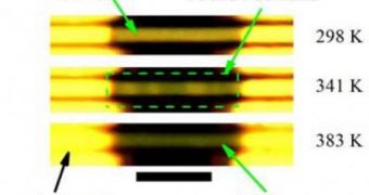
US Department of Energy's (DOE) Lawrence Berkeley National Laboratory (Berkeley Lab) experts have recently taken a crucial step in advancing the fields of magnetoresistance and high-temperature superconductivity research, when they have finally answered one of the elusive questions in physics today. The team has managed to determine precisely how placing strains on nanocrystals can change their electronic phases and their spatial arrangements, two feats that are of tremendous use for the high-tech industry. Details of the find appear in the latest issue of the journal Nature Nanotechnology.
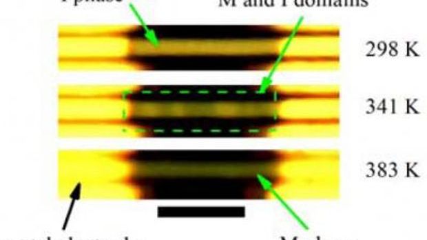
“By continuously tuning strain over a wide range in single-crystal vanadium oxide micro- and nano-scale wires, we were able to engineer phase inhomogeneity along the wires. Our results shed light on the origin of phase inhomogeneity in correlated electron materials in general, and open opportunities for designing and controlling phase inhomogeneity of correlated electron materials for future devices,” Berkeley Lab Materials Sciences Division physicist Junqiao Wu says.
The concept phase inhomogeneity refers to irregularities that appear in the micro-domain structure of correlated electron materials, he explains. Essentially, the team has learned that this phenomenon can be generated by external stimuli, such as applying strain on the materials. The expert, who also holds an appointment in the University of California in Berkeley (UCB) Department of Materials Science and Engineering, has also been the lead author of the new journal entry detailing the find, which is entitled “Strain engineering and one-dimensional organization of metal-insulator domains in single crystal VO2 beams.”
“This question is not only important for our understanding of the physics behind correlated electron materials, it also directly determines the spatial scale of correlated electron material device applications,” Wu says of the discovery. Spatial phase inhomogeneities, the scientist explains, are of major importance to the collective electronic behavior of correlated electron materials, but the question of whether they were caused by intrinsic properties of the materials, or by external stimuli, has remained unanswered until recently.
“By applying an electric field, the piezoelectric material would strain the correlated electron material to achieve a phase transition that would give us the desired functionality. To reach this capability, however, we will first need to design and synthesize such integrated structures with good material quality,” Wu concludes.

 14 DAY TRIAL //
