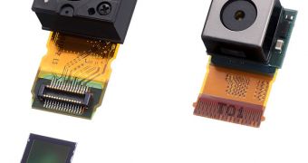
Sony has just announced that the company plans to invest $1.2 billion in its image sensor production facilities, enabling it to double the number of such sensors built, in order to keep up with the increased smartphones and digital camera demand.
This amount translates to 100 billion yen, part of the sum following to be subsidized by the Japanese government that runs a special program for helping environmentally friendly companies invest in their businesses.
All the money will go into CCD and CMOS image sensors facilities, Sony's goal being to double the production capacity of such chips.
According to the company, the investment plan includes the transfer of the semiconductor fabrication facilities from Toshiba (that were recently bough back by Sony), refurbishment of a part of this semiconductor fabrication facilities into new wafer lines capable of manufacturing CMOS image sensors as well as refurbishing a part of the production facilities at Nagasaki TEC Building 3.
The investment will further strengthen Sony's production capacity for Exmor and Exmor R CMOS image sensors, the Japanese company expecting to build approximately 50,000 wafers per month by the end of March 2012, compared to the 25,000 wafers that it builds now.
Exmor is the name of the technology employed by Sony in most of their CMOS sensors that performs the required analogue to digital conversion right on chip.
In addition, this technology also reduces the amount of noise present in an image and can be used in compact devices such as smartphones and digital cameras as well as in the larger APS-C sized sensors featured in DSLRs.
As for Exmor R, this is the name of Sony's backside illuminated sensor technology employed by the company in high-density sensors for compact cameras and cellphones.
At this time, Sony is the second largest digital camera manufacturer, the top spot being held by Canon, although this could change once this investment is finalized.

 14 DAY TRIAL //