14 DAY TRIAL //
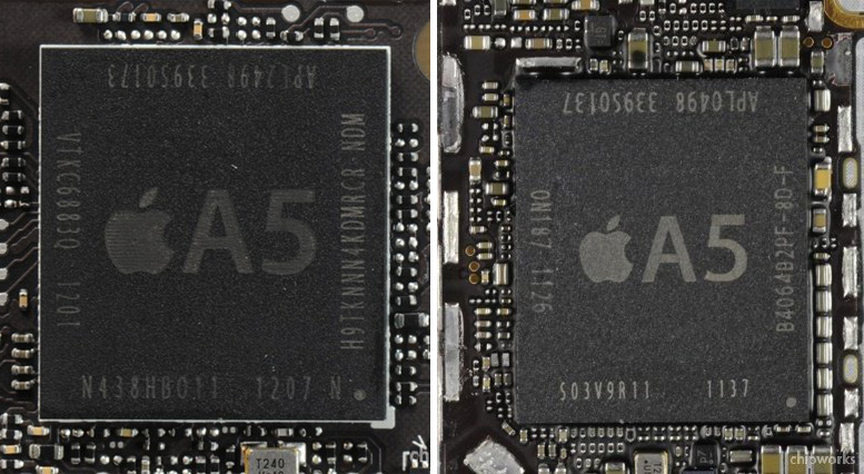
 Korean company Samsung has started mass production of Apple’s A5 ARM processor that powers the company’s popular iPAD 2 tablet. The move will have a serious impact on Apple's per-chip cost, but, more importantly, it proves once again how important it is to have a contract with a modern foundry using a quality manufacturing process.
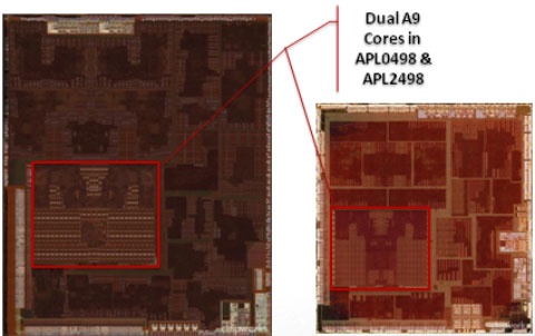
The old dual core A5 CPU was also manufactured by Samsung’s FAB, but the manufacturing technology was 45 nm.
The impact of moving A5 from 45nm to 32 nm is tremendous. Apple never wanted more performance or more features, like other CPU designers offer when moving to a smaller manufacturing process.
They wanted better chip costs and got a lower power consumption practically for free.
Better manufacturing costs derive from the fact that a 32 nm wafer containing 32 nm A5 dies will result in 200% more CPUs.
Of course, not all the CPUs will be perfectly functional and scalability is never perfect, but Samsung managed to get quite close to complete scalability.
Unlike most IC CPU design companies like AMD, Nvidia and Apple, they don’t usually pay for every working chip on a wafer, but for the processed wafer itself. Thus, Apple now pays likely close to the same amount of money for double the number of processors.
We have previously talked about reduced power consumption. For Apple’s iPAD this resulted in an almost 30% longer battery life when the CPU and iGPU is most intensely used.
Samsung's new 32 nm process has been in development since 2010 and Apple's A5 processor is the first truly mass-produced processor using the Korean company's new manufacturing process.
Here are some particular enhancements that Samsung is promising its FAB clients:
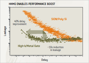
2x gate density increase compared to 45nm Over 100x lower gate leakage Greater than 40% delay improvement at fixed leakage 10X leakage reduction at fixed speed
Considering that Samsung’s own Exynos quad core ARM Cortex A9 CPU is made using the same process, we can easily see why Samsung’s 32 nm manufacturing capacities are more desirable than TSMC’s current 40 nm process.
Sure, TSMC is already manufacturing advanced chip in 28 nm technology, but the Taiwanese foundry cannot offer the same production volume Samsung does.