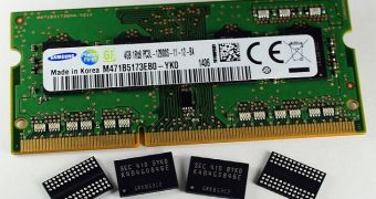
Toshiba may already be using a 19nm process technology, but the products made on it are NAND Flash chips, not DRAM. And with no one boasting a similarly high-tier technology, Samsung's latest DRAMs can be safely called the most advanced.
Sure enough, Samsung itself calls is the “most advanced DDR3 memory, based on a new 20 nanometer process technology, for use in a wide range of computing applications.”
Tech scaling is harder than for NAND, you see, because in DRAM, each cell consists of a capacitor and a transistor linked to one another (NAND only have the transistor).
The new chips are 4 Gb DDR3 DRAMs featuring modified double patterning technology, as well as ultrathin dielectric layers of cell capacitors with an “unprecedented uniformity.” This allows for higher cell performance.
Thus, manufacturing productivity has gone up 30% compared to 24nm DDR3, and over 100% compared to 30nm.
What's more, the 20nm 4 Gb DDR3 DRAMs are 25% more energy efficient than 25nm ones. A true victory for green technology if ever there was one.
Samsung's 4 Gb DDR3 chips should soon be used in everything from phones and tablets to DIMMs, SO-DIMMs and other such modules. No doubt some high-end memory maker or another is already preparing to reveal a DIMM set, maybe part of a gaming line or some such.

 14 DAY TRIAL //