14 DAY TRIAL //
 Silicon conversion from a disordered state to an ordered one can usually be carried out at temperatures as high as 700 degrees Celsius, which disables the possibility of applying silicon substrates on materials such as plastic or paper, due to enhanced heat sensitivity. Max Planck Institute of Metals Research scientists on the other hand claim to have found a way through which they can crystallize silicon at any temperature ranging between 700 to 150 degrees Celsius.
By applying a thin layer of aluminum on amorphous silicon, they were able to deliberately control the temperature at which silicon crystallizes, thus by lowering the crystallization temperature silicon semiconductor can now be applied on heat-sensitive materials. The study will probably be extended into developing a method through which the amorphous silicon can be prevented from changing into crystalline silicon, as both amorphous and crystalline forms are used in the semiconductors industry.
The fact that the crystallization temperature of a semiconductor can be altered in the presence of another metal has been known for a long time.
"We have exploited this effect for the first time in order to set the crystallization temperature of silicon using a covering layer of aluminum crystals," says Lars Jeurgens, from Eric J. Mittemeijer's department at the Max Planck Institute of Metals Research. Through this technique, it may be possible to create 20 nanometers thick silicon layers, at temperature as low as 200 degrees Celsius.
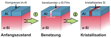
The crystallization temperature is directly dependent on the thickness of the aluminum layer and the ratio of energy between the silicon and aluminum layers. In order to save as much energy as possible, the silicon atoms must first be in a disordered state at the aluminum grain boundary, so that the two crystal lattice interfaces fit easier with each other. On the other hand, if the silicon were in an ordered state, the energy consumption would require to break the surface tension between the two would rise significantly.
The second phase of the interaction is consumed as silicon atoms start to arrange themselves into an ordered structure, which leads to an even further decrease in energy input. Because energy ratio between the two layers influences the temperature at which the crystallization process occurs, researchers are able to manipulate it by simply varying the thickness of the aluminum layer.
The study however covers only the start of the crystallization process, and does not explain what happens during the crystallization itself. According to Jeurgens, crystalline silicon will start to displace the aluminum layer, while aluminum atoms will travel through the silicon crystal and gather at the bottom of the block, but scientists haven't been able to understand why this happens.