14 DAY TRIAL //
 After being overclocked to 1.7GHz using liquid nitrogen at the beginning of this year, AMD’s Radeon HD 7970 graphics card has now reached a just as impressive 1.3GHz core frequency using only air cooling.
This feat was recently achieved by a Chinese enthusiast during a local overclocking contest, which took place earlier this week, reports Hardcore Hardware.
In order to reach this high frequency, the graphics card, which was provided by HIS, was stripped of its regular cooler and paired together with the Deep Cool Dracula VGA heatsink.
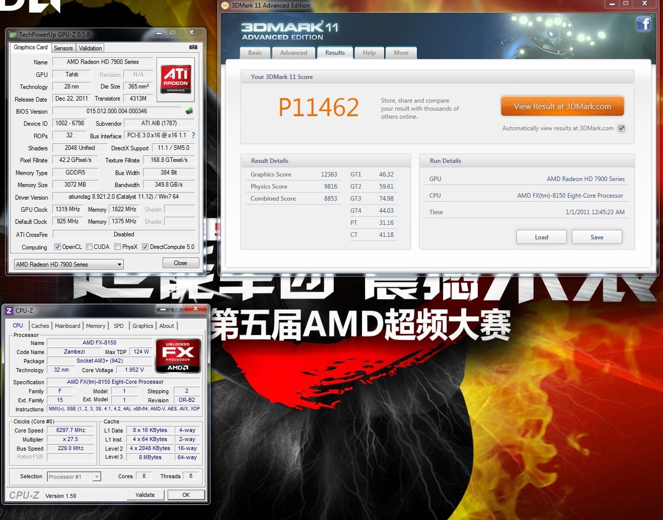
The GPU voltage was also increased, which allowed the card to be clocked at an impressive 1.319MHz, while the memory was pushed to 1,822MHz (equivalent to 7,288MHz).
Using these settings, the card was put through a series of 3DMark 11 runs where it managed to score an impressive P11462 using the Performance preset.
To put things in perspective, in the stock Radeon HD 7970, the graphics core is clocked at 925MHz, while the 3GB of GDDR5 video buffer memory runs at 1.375GHz (5.5GHz effective).
Besides the HIS Radeon HD 7970 graphics card, the rest of the system used for this overclock comprised an AMD FX-8150 processor, a Gigabyte AM3+ motherboard and a Corsair AX1200 PSU.
AMD’s Radeon HD 7970 was introduced by AMD in December last year and is based on the company’s Graphics Core Next (GCN) architecture.
At its heart there stands the Tahiti XT core, which includes 32 Compute Units for a total of 2048 stream processors that are joined by 128 texture units, 32 ROP units and a 384-bit wide memory bus.
All the hardware logic that AMD had to cram into this GPU, makes Tahiti XT the largest graphics core ever built, since it features no less than 4.31 billion transistors packed inside a 365mm2 die fabricated using TSMC’s 28nm High-K process.