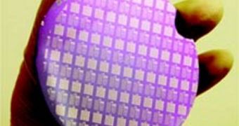
In spite of the massive amount of work that has been placed into making carbon nanotubes a standard material for our civilization, creating flexible arrays using the nanostructures has proven to be extremely difficult until now. The structures have the ability to innovate, among other things, the display control circuit technology. The arrays that feature carbon nanotube are more flexible than silicon, and also more efficient at doing their jobs. For the first time ever, scientists at the University of Southern California (USC) have demonstrated large arrays of fully functional nanotubes.
According to Technology Review, the team used simple and easy methods of producing the arrays, which were derived from batches of CNT that were impure. Scientists explain that today each pixel on the LCD screen of a computer is controlled by a number of transistors, which are generally made out of silicon, and fashioned into arrays. The latter need to be constructed inside vacuum chambers, at high temperatures, which makes the end-product very simple. However, replacing these arrays with CNT ones presents other challenges.
“Many people use one nanotube to make a very small, high-performance transistor,” USC Associate Professor of Electrical Engineering Chongwu Zhou, who is also a researcher on the new project, says. “If we use one nanotube for one transistor, the yield will never be high enough” to satisfy the requirements needed for mass-producing big screens. Zhou is convinced that replacing this approach with his team's may result in better devices. He explains that making larger transistors from mats of nanotubes could solve both the performance and the price issues.
The solution-processing technique that results in the USC nanotubes takes place at room temperature, the expert adds, which means that the prices go down incredibly since the very first step of the process. For their proof-of-concept, the experts designed and constructed a four-inch, carbon nanotube-laden silicon wafer, which they then successfully used to control a simple LED display. Details of the amazing work appear in the latest online issue of the journal Nano Letters.

 14 DAY TRIAL //