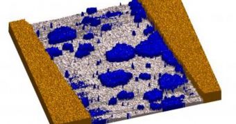
Self-assembled monolayer field-effect transistors (SAMFET) are among the latest developments of the relatively new plastic micro-electronics technology. These structures are constructed on organic materials, and also feature electronic components. Creating this type of transistors in a way that is both cost-effective and efficient was a long-pursued goal, which was recently achieved by an international cooperative effort by scientists from the Netherlands, Russia and Austria.
The team was able to determine for sure that monolayer coverage and channel length were two of the main factors that triggered the mobility of SAMFET devices, a find that could in the future lead to the creation of far more effective chemical sensors and similar instruments. Details of the find are published in the latest advanced online issue of the respected scientific journal Nature Nanotechnology. Most of the work was conducted at the Philips Research Eindhoven and Eindhoven University of Technology, in The Netherlands.
Philips Research managed to construct a SAMFET in 2008, based on a silicon substrate, which was then immersed into a solution containing liquid crystalline molecules. These molecules self-assembled on the substrate, and the end result was a semi-conductive layer of just a single molecule thick. Experts say that the monolayer features up-standing molecules, a fact that allows conduction to take place by “jumping” from one to another.
But scientists working on this project noticed that, as the length of the transistor increased, its conductivity level decreased exponentially, in a very counterintuitive manner. After a great deal of study, done at the University of Groningen, the Holst Center, the Enikolopov Institute for Synthetical Polymer Materials, in Moscow, and the Technical University in Graz, Austria, the team understood that the monolayer coverage was the main element that caused this to happen.
A simple percolation model made everything clear. The scientists compared the transistor to a river, which the current passes by jumping from one bridge (molecule) to another. If the distance between them increases, then the process becomes more difficult. And this is precisely what happened when the size of the SAMFET increased. The molecules became separated to such extents that it was immensely hard for electrical currents to “jump” from one to the other.
“If we go back to that river again, another benefit of a SAMFET becomes clear. Imagine that there are just enough rocks to cross that river. When you remove just one rock, the effect is significant, for it is impossible to make it to the other side of the river. The SAMFET could be used to make sensors that give a large signal that is triggered by a small change,” explains Eindhoven University of Technology assistant professor Martijn Kemerink.

 14 DAY TRIAL //