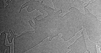
Since it was first discovered in 2004, graphene has proven to be one of the most promising new materials in the world, having the potential to be used for new generations of semiconductors and other components of innovative electronic equipment. Now, a group of research institutions has managed to create interconnected carbon nanostructures using the material as a substrate, which may bring these classes of electronics a step closer to reality.
The result of a collaboration between scientists at the University of Pennsylvania, the Sandia National Laboratories (SNL), and the Rice University, the accomplishment is nothing but a simple assembly process, but which is done at the nanoscale. For the structures to be created, graphene sheets, only a few atoms thick, are heated to sublimation using electrical current, and then maneuvered in their positions. The scientists in the team came to the conclusion that it would be a lot faster and cheaper if carbon nanotubes were grown directly from the graphene substrate.
If they were to be grown separately, the experts would have come across the same problem that all other groups looking into nanotubes do – the fact that they are simply too small to be picked up and handled without damaging them. So, as the possibility to use graphene as a substrate arose, they used it, and for good reason. If edges are cut in graphene, and other sheets of graphene are placed alongside it, then the edges on the two bind to each other so seamlessly, that no one can tell where the joining is. The team has likened the process to what comes out of the hands of a skilled welder, who fits pipes together perfectly.
“This study demonstrates it is possible to make and integrate curved nanostructures directly on flat graphene, which is extended and electrically conducting. Furthermore, it demonstrates that multiple graphene sheets can be intentionally interconnected. And the quality of the plumbing is exceptionally high, better than anything people have used for electrical contacts with carbon nanotubes so far. We are currently investigating the fundamental properties of graphene bi-layer edges (BLE), BLE rings and nanotube-BLE junctions,” Penn State Department of Materials Science and Engineering Material Scientist and Associate Professor in the School of Engineering and Applied Science Ju Li says.

 14 DAY TRIAL //