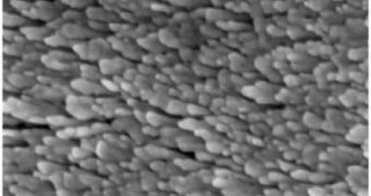
According to scientists in the field, one of the basic requirements for advancing the 3D-chip technology is growing appropriate nanorods, which are the basic components of these types of circuits. These products have to be as “sticky” and slim as possible, so as to fit more of them in a tight place, without clogging them together too much. Now, a team of researchers at the Rensselaer Polytechnic Institute in New York seems to have cracked this mystery by developing a new method of growing these copper nanorods to certain specifications.
The temperature at which nanorods fuse together, or anneal, is entirely dependent on the rods' thickness. The thicker they are, the higher the temperatures required to melt them must be. But the new method developed at the RPI only needs some 300 degrees Celsius to do this, which is relatively low.
This significantly reduced temperature is only possible due to the fact that the rods themselves are very, very thin, even for the nano-scale. This makes them ideal for “stitching” together the stacked nano-components required to create 3D processing chips.
“When fabricating and assembling 3D chips, and when bonding the silicon wafers together, you want as low a temperature as possible. Slimmer nanorods, by virtue of their smaller diameters, require less heat to anneal. These lower temperatures won't damage or degrade the delicate semiconductors. The end result is a less expensive, more reliable device,” RPI Center for Integrated Electronics research associate Pei-I Wang explains.
RPI R.P. Baker Distinguished Professor of Physics Toh-Ming Lu is the expert that has led the team into the new technology and also the author of a paper detailing it, published in the scientific journal Nanotechnology.
Another team has also studied the ways in which these slimmer rods can be integrated in the construction and bonding process of silicon wafers, which will make up the future 3D chips. The second study, led by RPI Center for Integrated Electronics (CIE) associate professor James Jian-Qiang Lu, has been published in the latest issue of the journal Electrochemical and Solid-State Letters. Lu is also an associate professor at the Institute's Department of Electrical, Computer, and Systems Engineering (ECSE).

 14 DAY TRIAL //