14 DAY TRIAL //
 Back when the Santa Clara, California-based graphics chip maker NVIDIA first announced its GT200-based graphics cards, the green company initially introduced two different models, namely the GTX 260 and the GTX 285. These two cards were designed for the mainstream and high-end maker segments, enabling users to the take advantage of the company's 65nm-based graphics processor.
However, from the two, the GTX 260 model is the one that has gone through the highest number of modifications, becoming the first GT200-based card that featured a 55nm GPU. It now appears that NVIDIA is planning another change for its GTX 260 graphics card.
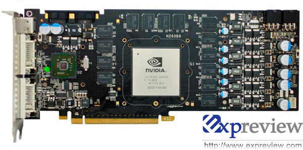
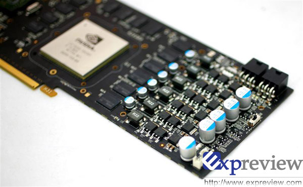
According to details made available by Expreview, the chip maker is planning to change the PCB of its mainstream GeForce GTX 260 graphics card, in an attempt to reduce costs and still provide the customer with one of its most successful cards. This third-generation GTX 260 design plan boasts NVIDIA's new P897 PCB design. This features a 4/6 phase NVVDD power solution ADP4100 and changes the FBVDDQ power solution from 2-phase to single phase. In addition, the MOSFET package has been changed from LFPAK to DPAK, in an attempt to save costs, while the PCB layer decreased from 10 to 8.
The card will continue to feature the same length, but the company has decided to reduce its height by 1.5cm. According to Expreview, the green company may try to change the DVI connector and reduce the BIOS Rom from 1M to 512K, to further cut costs. All the aforementioned design changes are expected to reduce the card's manufacturing costs by $10 to $15, which will likely reflect in its pricing, when it becomes available next month.
The current P654 reference design has also been enabled to further reduce costs, when compared to the card's initial P651 reference design.