NVIDIA should be able to launch its next-generation card line in April, which means that bits and pieces of info on it will only leak to the net faster.
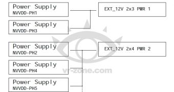
It is thermal design power that has managed to raise some questions most recently, due to the power distribution diagram.
Normally, a reference high-end board should be capable of working on just two six-pin PCI Express power connectors.
The diagram suggests that the Kepler won't be satisfied with just that much: it includes one six-pin PCI Express connector and an 8-inch plug.
That means that, in addition to the 75W provided by the PCI Express slot and the 75W of the 6-pin plug, there are an extra 150W to use.
Three phases are tasked with supplying energy to the GPU itself, while the remaining two power the rest of the add-in-board: 2 GB of GDDR5 VRAM and whatever third-party chips exist (NVVDD-PH1 and PH3).
We've been keeping track of all the info surfacing about the next-generation NVIDIA graphics products.
What we know, among other things, is the CUDA design, the general specs and even the traits of the GeForce GTX 670 Ti, the strongest models powered by the GK104.
The news about Kepler possibly having a 300W TDP is not as encouraging as the rest, since it is a fairly high mark, especially for these times when the emphasis on power efficiency is at its highest.
Granted, customers likely to choose the upper-end boards probably have power supplies that can handle the load easily (500W+).
Nevertheless, when compared to the rated TDP of the AMD Radeon HD 7970 (250W), we cannot help but raise a curious eyebrow.
Then again, the Santa Clara, California-based company has been painting the Kepler as being a much stronger graphics chip than anything AMD has, so the extra power is probably a necessary compromise.

 14 DAY TRIAL //