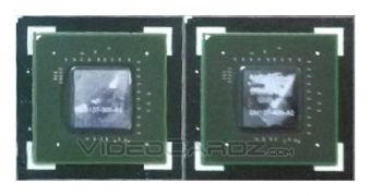
Information about the GM107 Maxwell graphics processing unit from NVIDIA has been slowly trickling into sight over the past few weeks, and at this point, the only relevant thing we don't know about it is the TDP (thermal design power).
The first die shot of the Maxwell chip has been posted by VideoCardz, along with a full list of the chip's specifications.
There will, apparently, be two iterations of the chip, called GM107-300 and GM107-400, with the only differences between them being the CUDA core and TMU counts (texture mapping units).
Thus, we may as well assume that the GeForce GTX 750 that is scheduled for release later this month won't be alone for long.
Or maybe the GM107-300 will be used for a mobile GPU of some sort, while the GM107-400 will power the desktop card everyone's been dying to finally see.
Anyway, the GM107 maxwell chips will both be designed on the 28nm micro-architecture, even though NVIDIA intended to move to 20 nm by this point. Sadly, TSMC isn't ready to manufacture 20nm chips yet.
Considering that, it's more understandable that NVIDIA would not call this board GeForce 800 series. 800 is reserved for the “true” Maxwell that will debut later this year.
That said, the GM107 is still 30% smaller than the GK106, and needs a lot less power than any Kepler GPU, to the point where the GTX 750 could work without 6-pin or 8-pin power ports (NVIDIA will include one anyway though).
All in all, the 28nm Maxwell could be labeled as a refresh of the Kepler with much higher efficiency.
The GM107-300 has 768 CUDA cores, 64 TMUs, 16 ROPs (raster operating units) and a memory bus of 18 bits.
The GM107-400 is similar, but has 960 CUDA cores and 80 TMUs. Its TDP should be of around 75W, which means the GM107-300 might have the same.

 14 DAY TRIAL //