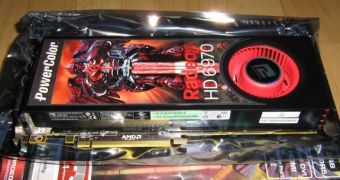
The past few weeks have not been too poor in leaks and reports regarding AMD's newest upcoming cards, and it seems that the role of a certain element on the HD 6970 has finally been discovered.
Most of the performance details of the AMD Radeon HD 6970 have been already leaked to the web, along with such photos as those of the unboxing of the PowerColor version.
Based on those photos, as well as whatever other pictures of the board have made it to the web, some have noticed the existence of a switch next to the Crossfire connectors.
Now, it appears that Fudzilla has discovered the purpose of said switch, a purpose that may get overclockers especially excited.
What that switch does is allow the user to choose which of the two BIOSes to activate.
Indeed, the card has dual-BIOS, one setting being protected as factory default while the other one is meant for user customization.
Basically, setting 1 of the switch activates the unprotected BIOS. This BIOS is the one that users can update and use in their tweaking and overclocking tasks.
The second setting is a failsafe of sorts, being protected as factory default, or so says the report.
For those in need of a reminder, the AMD Radeon HD 6970 has 1,536 Stream Processors, 2 GB of GDDR5 VRAM, a memory interface of 256 bits and 96 texture units.
The graphics processing unit operates at a frequency of 880 MHz, while the memory has a clock speed of 5,400 MHz.
So far, it is not completely clear whether AMD releases a BIOS that boosts performance while raising power consumption, or if the customizable BIOS has some other purpose.
Either way, all will become clear on December 15, since that is when the official launch of the card is set to take place.

 14 DAY TRIAL //