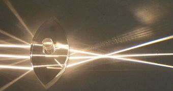
Experts from the Northwestern University Electronic Materials Research Institute, led by Director and Distinguished Professor Srinivas Sridhar, PhD, announce that they were able to produce a new type of lens. The device, which is built at the nanoscale, operates in such a manner that it exceeds the diffraction limit, a classical limitation that holds that no type of lens can see details that are smaller than half the wavelength of the light doing the imaging. If the observations are done in visible light, then the size of the objects cannot be larger than a few hundred nanometers. However, the NU group argues that super-resolution imaging is possible, and that their nanolens is capable of it, PhysOrg reports.
The researchers reveal that the nanolens itself is created out of an array of artificially engineered nanowires. These structures are known as metamaterials, because they cannot be found in nature. They are constructed specifically to handle the photons inside light in very special ways. Additionally, metamaterials also make use of the dual nature of light (particle and wave at the same time). The overall result is a lens with imaging capabilities that are superior to anything else capable with the current technology, the NU group says.
Regular lenses, in the form that we all know them, only handle the ordinary waves of light. These reflect off the surface being observed, but do not carry with them the finest details. This translates in practice into the fact that very small details cannot be observed using light-based microscopes. But what the research group did was elaborate on a method of also taking into account the action of evanescent waves. These waves carry with them a lot more information about the fine structure of things, but unfortunately they decay very fast, in an exponential correlation to the distance they travel away from the surface that created them. They generally tend to be most intense within one-third of a wavelength from the surface that generated them.
In the NU approach, the nanolens is a lens only by name, as it bears no similarity to a normal lens. There are millions of nanowires placed in very specific patterns on a substrate, and each of the structures is just 20 nanometers in diameter. Their disposition is what allowed the physicists to control the motion of light through the device, and as such obtain as much detail of the target object as possible. Among the fields of science that stand to benefit most from this type of innovation are biomedical imaging technologies and lithography methods, widely used in the electronics industry.
“This is the best superlens realized so far and is a significant development in the field of high resolution optical imaging. We have the capability for the large-scale production of these nanolenses and hope to manufacture these devices in the near future,” Sridhar says.

 14 DAY TRIAL //