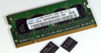
Following the GDDR4 4GB/s boost, Samsung Electronics sets the trend once again with the introduction of the first mass production 60nm 1Gigabit (Gb) DDR2 DRAM.
The 60nm manufacturing technology raises the bar, increasing production efficiency by 40 percent over the previous 80nm fab process that was integrated into DRAM modules back in early 2006. 90nm general process technology that is in use in today's entry-level and mainstream hardware devices is two times less productive than the new 60nm process.
Samsung predicts that, with the adoption of its latest 60nm process, 1Gb DRAM chips will further increase the demand for large density DRAM modules, complementing the minimal memory requirements of at least 1GB imposed by Windows Vista. Samsung offers 512MB, 1GB, and 2GB densities for the new 60nm chips, which can be clocked at either 667MHz or 800MHz speeds.
The migration to nanometer technologies has brought the integration of three-dimensional (3D) transistors to build increasingly smaller chips. 3D transistors heavily rely on a recess channel array transistor (RCAT) that actually constructs the DRAM cell three-dimensionally to minimize its size while increasing its density. This key component is expected to enable DRAM fabrication to 50nm and below. Moreover, Samsung uses a special metal-insulator metal (MIM) for improved capacitor stability.
Another included technology that boosts the overall DRAM performance is the use of selective epitaxial growth (SEG) methods, which provide a broader electron channel, and optimize the speed of each chip's electrons to reduce power consumption and enable higher performance.
The 60nm process is expected to completely replace the mainstream 90 nm circuit technology for DRAM by 2008. For the first year of 60nm chip availability (2007), Samsung expects revenues of around US $2.3billion worldwide, with as much as US $32 billion by 2009.

 14 DAY TRIAL //