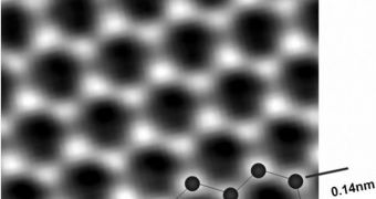
Since 2005, when experts at the University of Manchester discovered the carbon compound known as graphene, the international scientific community has been convinced that it found the replacement material for silicon. But experts are well aware that they need to understand graphene thoroughly before using it in mass, and recent studies show that science is barely beginning to scratch the surface of what graphene can do. Just recently, investigators learned that the material can be stretched in a way that produces “nanoscale bubbles” on its surface, CleanTechnica reports.
Numerous American researchers are part of the national US effort to make sense of graphene. Generally, the material can conduct electricity very well, but a few manipulations can turn it into either a semiconductor or an insulator. Several universities and research institutes around the country are working on creating combinations of graphene and various other materials, and results are starting to show.
For example, researchers at the University of South Florida (USF) are working on ways of rolling graphene into nanowires, in an investigation supported by the US National Science Foundation (NSF), while experts at the Rice University are studying possible ways of using grapahane as an insulator. This material is closely related to graphene, but has different properties. At the University of Chicago, water droplets are used to produce various modifications in the natural shape graphene takes on. It was there that chemists made an accidental finding with potentially far-reaching implications.
The UC team used a platinum crystal as a substrate for growing the carbon compound, not knowing that subjecting it to the influence of the crystal would hinder the development of the atom-thick, honeycomb-like lattice that makes up graphene. Triangular nanoscale “bubbles” developed, which apparently did not have the same energy levels as the rest of the graphene sheet. When experts measured their properties, their energy levels spiked well above the mean ones in the material.
Researchers at the Massachusetts Institute of Technology (MIT) took this accomplishment even further, when they demonstrated that the growing method can be applied to other materials as well. They emulated the procedure by applying a phenomenon called lattice strain to yttria-stabilized zirconium. The material soon developed the nanoscale “bubbles,” which proved to conduct electricity four orders of magnitude better than the unmodified material.

 14 DAY TRIAL //