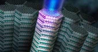
Working together, experts from the Arizona State University, in the United States, and the Technical University of Eindhoven, in the Netherlands, have recently developed new methods of creating even smaller lasers, to be used in applications at the nanoscale. Existing methods are very cumbersome to follow, and require a lot of work and resources to produce a viable nanolaser. Reporting in a recent issue of the online science and engineering journal Optics Express, the team says that the new instruments will be an important part of the communication systems inside computers in the future.
They also add that the size of the laser is a very important factor in determining the level of miniaturization that certain electronic components can have. This was also made apparent in an unrelated study we reported on earlier, in which a mass spectrometry device at the nanoscale could not be implemented because the related nanowire technology did not yet exist. In the new experiments, the researchers realized that using increased numbers of lasers in the same tight processor, for example, could significantly boost its power and capabilities.
However, up until this point, scientists working with lasers from all over the world believed that the minimum size of such an instrument could be only half of the observed frequency. To put things into perspective, consider the fact that your average communication laser, used to power fiber optic cables crossing the world's oceans, works on a 1,500-nanometer wavelength. This means that the device itself can be no smaller than 750 nanometers. The new research proposes that this limitation – called the diffraction limit – can be overcome.
“It turns out that the electrons excited in metals can help you confine a light in a laser to sizes smaller than that required by the diffraction limit. Eventually, we were able to make a laser as thin as about one quarter of the wavelength or smaller, as opposed to one half,” ASU Ira A. Fulton Schools of Engineering School of Electrical, Computer and Energy Engineering Professor Cun-Zheng Ning, who has been the team leader for the American researchers, explains.
“This is the first time that anyone has shown that this limit to the size of nanolasers can be broken. Beating this limit is significant. It opens up diverse possibilities for improving integrated communications devices, single molecule detection and medical imaging. Nanolasers can be used for many applications, but the most exciting possibilities are for communications on a central processing unit (CPU) of a computer chip,” he adds.

 14 DAY TRIAL //