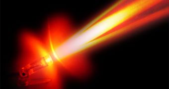
Gallium-arsenide semiconductor material is to optoelectronic devices much like silicon to computer microprocessors and microchips. However, while silicon processes electronic signals, gallium-arsenide is used to convert electric energy into light. Basically, any light emitting diode and LED laser works on the basis of a tiny gallium-arsenide semiconductor chip.
The tendency today is to boost the electric energy to light conversion ration, thus making gallium-arsenide based lighting sources more efficient. One way to do so it to increase the brightness of the electroluminescent device. University of California researchers reveal that they have been able to the light output of a gallium-arsenide structure by pumping light into needle-like nanostructures measuring 3 to 4 nanometers in length and 2 to 5 nanometers across, disposed at angles between 6 to 9 degrees from top to bottom.
It is the first time when researchers use a defect-free gallium-arsenide crystal substrate, without the use of catalyzers. The next step, says leader of the research Michael Moewe, is to turn these tiny needles into lasers. Because the sharp tips of the needles can be produced without the need of further etching or processing steps, Moewe believes that they could be of value of applications such as atomic force microscopy (AFM), which can create atomic resolution image of a particular surface. AFM may also represent a new technique of data storage, by influencing the atoms on the surface of the scanned sample.
Alternatively, Raman spectroscopy may also be enhanced by making used of such nanostructures. Through the Raman spectroscopy techniques, researchers are able to measure the energy levels of molecules by simply shinning them with a light beam of known frequency, than measuring the frequency of the reflected light. With the use of sharp tipped nano-needles, one could in theory measure a single molecule.

 14 DAY TRIAL //