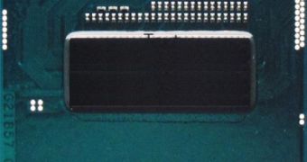
Intel is the world’s largest semiconductor company. Unlike AMD, Intel has its own FABs and, for quite a number of years, the company enjoys a manufacturing process advantage along with an architectural advantage over its main competitor.
Therefore, Intel already has its next-generation processors available and running, but for profit reasons, the company is only going to launch them after another six or so months have passed.
Intel has already demonstrated the processors quite a number of times before and it is clear that the processors are ready or almost finished.
The company might want to work on better drivers and software to put that amazing Haswell iGPU to good use. We’ve reported here about Haswell’s impressive iGPU.
During Intel Developer Forum 2012, the company is reportedly going to discuss Haswell’s technological innovations along with the new 2nd-generation vector extensions, bit manipulation instructions and transactional synchronization extensions.
From what we know, Haswell will bring more than BMI, AVX2 and TSX, but AMD’s own next-generation Jaguar core will bring BMI support also.
The new processor will still use two DDR3 memory channels and will support DDR3 and DD3L memory. It will come with three PCI Express 3.0 controllers and a further refined Turbo Boost technology.
The integrated graphics processing unit is codenamed Denlow and this new architecture, besides increasing performance over three times like we reported here, it will also bring support for DirectX 11.1, OpenGL 3.2+ and some other improvements.
The company is already certifying its iGPUs for work with professional CAD applications and Ivy Bridge already has plans for ProEngineer, Maya, 3ds Max, Softimage XSI and others.
The thing is that Intel’s graphics, although relabeled as “professional,” display catastrophic performance like we’ve reported here.

 14 DAY TRIAL //