14 DAY TRIAL //
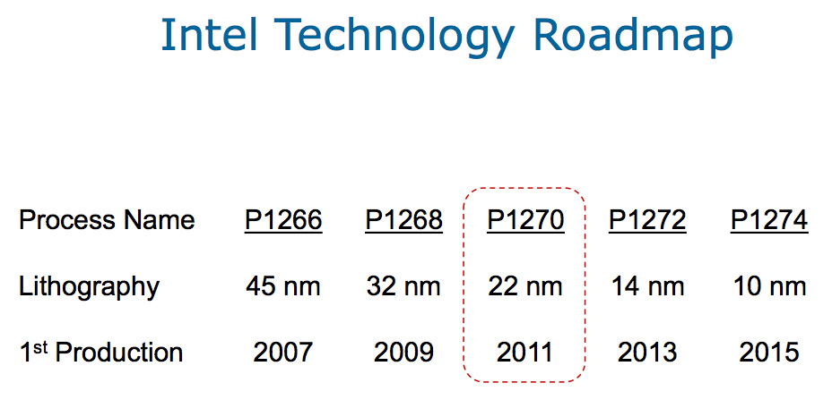
 Earlier today Intel announced that its upcoming Ivy Bridge processor will be the first high volume 22nm chip produced using 3D transistors, but the company has no plans of stopping here and wants to transition to the 14nm fabrication node as soon as 2013, while the 10nm process is expected in 2015.
Both of these new technologies will feature the Tri-Gate 3D transistor design which allows for more energy efficient processors to be built.
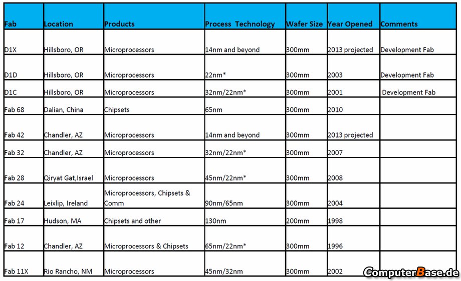
Right now, Intel's plans call for five of its 300mm wafer fabs to be converted to the 22nm manufacturing, but the company is also working on its schedule for the transition to 14nm.
To get ready for this change, Intel will built two new facilities which are going to be placed in Hillsboro, Oregon, and in Chandler, Arizona. Both are expected to start production by the end of 2013 and use 300mm wafers.
Just as the other facilities built by Intel in Hillsboro, the D1X 14nm fab will also be used for development purposes.
Moving forward in Intel's future, 2015 will mark the introduction of the company's 10nm fabrication technology, that is also known internally under the “P1274” process name.
The information available now about this node is rather sketchy, but both of Intel's 2013 fabs are “14nm and beyond” capable so these could be converted to 10nm in the not-so-distant future.
Intel is expected to start mass production of Ivy Bridge CPUs using the 22nm Tri-Gate process technology in the second half of this year.
Ivy Bridge is just a die shrink of the current Sandy Bridge architecture and brings a limited number of improvements such as better integrated graphics, with support for DirectX 11, better AVX and AES-NI performance, and PCI Express Gen 3.0 support. (via ComputerBase)