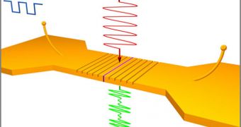
A group of physicists at the Stanford University announces the development of a new type of light source, which makes use of the power of plasmonics. The ultra-compact, nanoscale device may soon be used to underly the next generation of communications equipment.
Similarly, such advanced light sources could also be used to improve fundamental concepts in science, which currently cannot be expanded upon due to a lack of sufficiently-developed technology. The way to go forward has existed for decades, but thus far it has been impractical to take it.
What the research team did was take an electric-field-induced second harmonic light generation (EFISH) device, and miniaturize it to the nanoscale. Such a light source required thousands of volts to operate until now, as well as very large crystal and high-energy lasers.
An EFISH source makes use of second harmonic generation, an effect discovered in the 1960s. It manifests itself when a laser beam is shone through certain types of crystals, producing photons of a very different color, usually twice the original wavelengths.
Interestingly, physicists also determined that a similar effect – EFISH – could be obtained if an electrical field was applied to the crystals. But the beam of light produced in this manner was significantly less intense than the one produced through direct second harmonic generation.
As such, the electric-field-based method was set aside as a scientific curiosity, and not used except for some very specific applications. In the new study, the Stanford team took EFISH devices and made the smaller, all the way to the nanoscale. This makes them suitable for many new applications.
Details of the new, ultra-compact light source were presented in a paper published this week in the top journal Science. In the new device, “the light-matter interaction becomes nonlinear. The light you get out is different from the light you put in,” Alok Vasudev explains.
The study team member is a graduate student at Stanford, and also the coauthor of the new paper. He conducted the work with associate professor of materials science and engineering Mark Brongersma.
“Now, Alok and I have taken this knowledge and reduced it to the nanoscale. For the first time we have a nonlinear optical device at the nanoscale that has both optical and electrical functionality. And this offers some interesting engineering possibilities,” Wenshan Cai adds.
The expert, a postdoctoral researcher in Brongersma's lab, is also the first author of the Science paper.
“If you have two electrodes placed extremely close together, as we do in our experiment, it doesn't take many volts to produce a giant electrical field. In fact, it takes just a single volt,” Brongersma adds. “It is this fundamental science that allows us to shrink the device by orders of magnitude from the human scale to the nanoscale,” Cai concludes.

 14 DAY TRIAL //