14 DAY TRIAL //
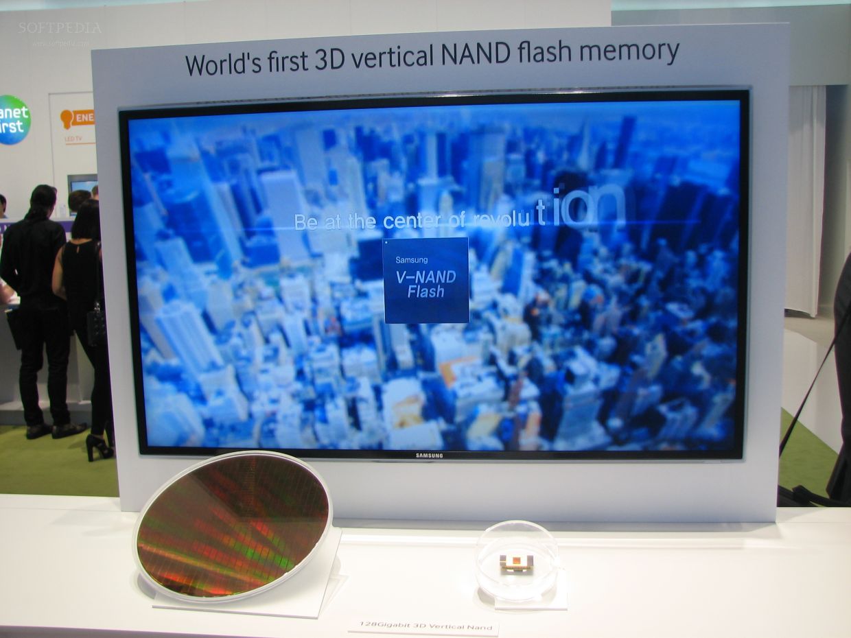
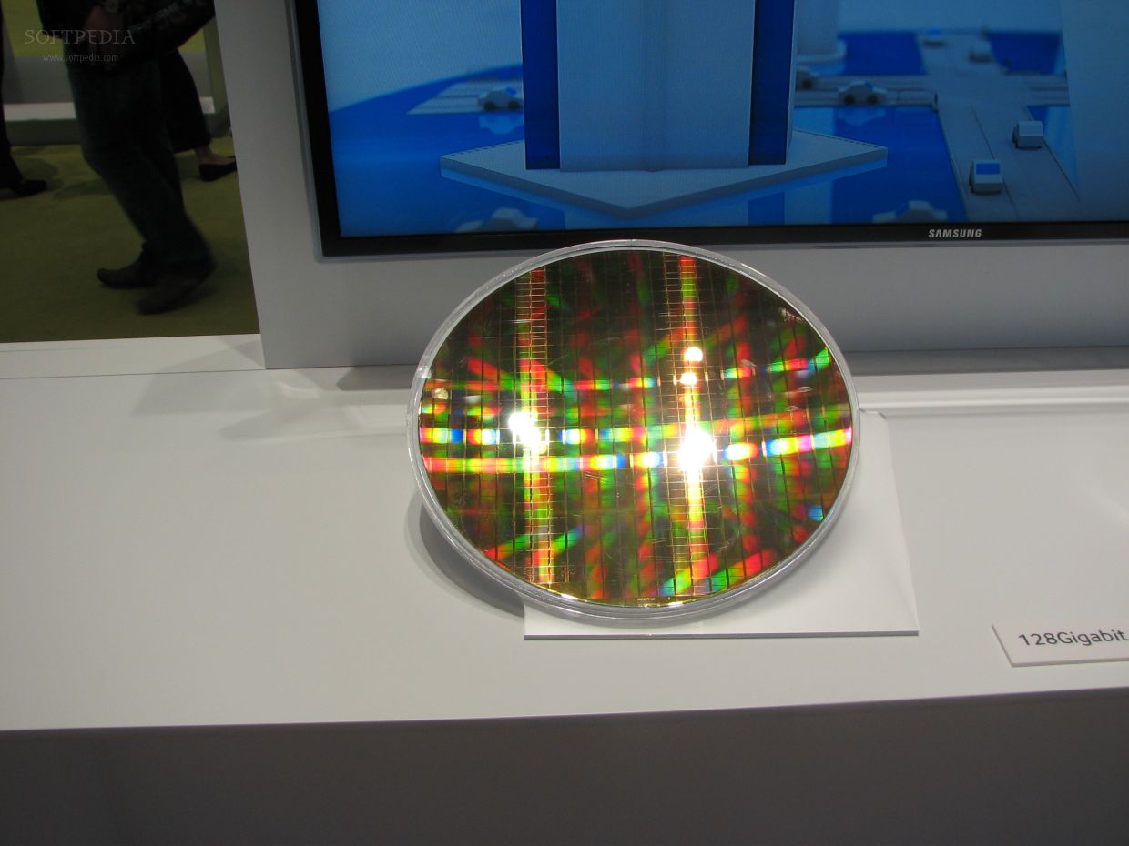
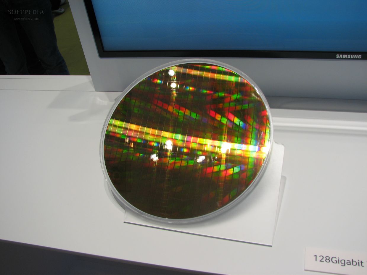
 Samsung's V-Nand technology is a type of memory chip that has twice the density of normal 20nm MLC NAND Flash chips.
That puts each chip at 128 Gb MLC, rather than 64 Gb MLC. Quite impressive, considering that another consequence of stacking chips is half the power draw.
More importantly, though, is that the layered call structure can go from 2 to 24 layers.
Add to that the V-Nand reliability of 2-10 times over that of previous-generation Samsung NAND Flash technologies, and you have something that anyone should love to own.
Sadly, Samsung is only offering SSD solutions for enterprise servers right now. Still, the company has promised that PCs will benefit from it too, eventually, so we just have to wait a bit before we get that twofold boost in writing speed, on top of everything else.