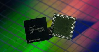
Hynix has been the first to introduce not one, but several types of DDR chips, with two of the more recent ones being last year's 54nm manufacturing process-based 1Gb DDR2 chip and the world's first 40nm-based 2Gb GDDR5 chip. Eager to introduce yet another in the 'world's first' series, Hynix Semiconductor has launched its latest product, the 40nm 2Gb DDR2 chip for use in mobile devices such as smartphones, smartbooks and tablet PCs.
The new memory chip is the fastest among the current mobile DRAM solutions, working at 1,066 Mbps (megabits per second). Not only is this speed the fastest, but the new DRAM also boasts a high density in Package on Package (PoP) or Multi Chip Package (MCP) types. The product meets the standards set by JEDEC and is part of Hynix's plan to maintain competitiveness in a diversified product line-up.
The 2Gb DDR2 is capable of operating on a voltage as low as 1.2V, even while using a 32-bit I/O, which provides a high bandwidth of 4,26 GB (Gigabytes) of data per second. The chip does this and still manages to consume 50 percent less power than other mobile memory solutions.
Hynix Semiconductor introduced its first 2Gb mobile DDR in 2008. That product was also a world's first and was built based on the 50nm-class process technology. This latest DRAM memory chip is partly aimed at enforcing Hynix's position on the global Mobile DRAM market. The company plans to continue to “capitalize on its technology leadership in the future.”
While no exact details have been given, the new 2Gb DDR2 DRAM built on the company's leading 40nm-class process technology is set to be pushed into mass production sometime during the first half of the ongoing year. The company will soon start making sample shipments.

 14 DAY TRIAL //