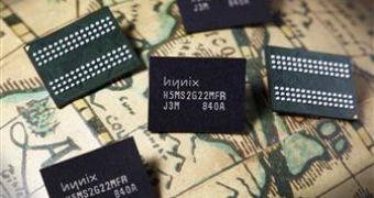
Hynix Semiconductor has just announced that it has successfully developed the world's first 2Gb Mobile DRAM using the 54nm technology. The company's solution will enable upcoming mobile internet devices (MIDs) and other small-sized, portable computer systems to deliver a higher capacity memory solution.
The product provides a considerable leap forward from the current 1Gb mobile solution, which, until now, has been the highest density offered among the mobile DRAM products in MCP (MultiChip Package) and PoP (Package on Package) platform.
The new product has been designed to deliver a high capacity level, as well as the kind of performance required by the next-generation of MID and UMPC (Ultra Mobile PC) systems. Basically, the new Hynix 2Gb Mobile DRAM is specified to provide a maximum operating speed of 400Mbps (Megabits per second), at a 1.2V power supply. That is enough to enable the memory to process up to 1.6 Gigabytes of data per second with a 32-bit I/O. Also, according to the company, its latest product has been specifically designed to provide a better power consumption level, when compared with existing memory solutions.
The 2Gb solution basically comes to provide a high memory density, low power consumption, fast operating speed and small size features. It meets JEDEC standard, making it suitable for upcoming MIDs and UMPCs, as well as for other products that require a higher density memory solution.
Additional features include the company's “One Chip Solutions,” which offers a flexible solution that has been designed to meet the specific needs of customers looking for both SDRAM and DDR DRAM interfaces, with both x16 and x32 organizations on a single chip.
The company has also announced that it plans to start mass producing the new memory solution in the first half of next year, coming to satisfy the increasing demand for high performance mobile applications.

 14 DAY TRIAL //