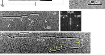
According to experts at the US Sandia National Laboratories (SNL), working together with colleagues from the University of Pennsylvania in Philadelphia, the Rice University and the Hong Kong Polytechnic University, graphene exhibits some pretty interesting properties when subjected to in situ Joule-heating inside a transmission electron microscope. The behavior is roughly similar and comparable to that of burning paper, which crumbles and twists, leaving behind ash that is bent.
In their study, the investigators noticed that several layers of graphene undergoing Joule heating behaved in very much the same way as paper did. “Imagine burning a piece of paper: The reaction front tends to be jagged. Furthermore, if one examines the ashes left behind, most are curved. This is because paper, being a thin 2-dimensional (2D) object, is easy to bend. Here, we report an analogous experiment, but on graphene instead of ordinary paper, and at the nanoscale inside a high-resolution transmission electron microscope (HRTEM),” the authors wrote in a new paper detailing the behavior, published in the June 23rd issue of the journal Proceedings of the National Academy of Sciences.
“We induced the sublimation of suspended multilayer graphene by Joule-heating, so it becomes thermodynamically favorable for carbon atoms to escape into the gas phase, leaving freshly exposed (open) edges on the solid graphene. The remaining graphene edges curled up under observation, and often welded together,” the team further explained. In charge of the research was SNL Center for Integrated Nanotechnologies expert Jian Yu Huang.
“We attribute this behavior to the driving force to reduce dangling bonds on the edges (capillary energy), at the cost of bending energy. The sublimation of few-layer graphene, such as a 10-layer stack, is particularly interesting compared with the sublimation of monolayer graphene. In few-layer graphene, different layers often spontaneously fuse together, forming nanostructures in situ, on top of 1 or 2 electrically conductive, extended, graphene sheets,” the team added in the PNAS report.
The team reported that engineering new types of integrated carbon-based devices could soon become a lot easier, thanks to the new finds. If the process of edge bending in graphene could be mastered, the experts said, then nanostructures could be built in a much easier way, and with less resources than until now, when they had to be generated through complex chemical processes.

 14 DAY TRIAL //