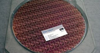
During a presentation that was held for members of the press last week in Dresden, GlobalFoundries has announced that it has already started the production of the first 300mm test wafers using the 28nm process technology.
These wafers are currently made up of simple circuits, like test patterns and SRAM macros, and the process isn't expected to become mature enough until late next year.
At first, the 28nm fabrication node will be used for producing SoCs (system-on-a-chip) and other such products, but, eventually, the process is going to be used for more complex parts, such as GPUs and CPUs.
For example, AMD plans to use it for the upcoming Radeon HD 7000 family of graphics processors.
All GlobalFoundries' 28nm technologies employ the Gate First approach to HKMG, which should deliver improved power efficiency when compared to other foundry technologies.
To get ready for the introduction of the 28nm manufacturing process, GlobalFoundries has announced at the beginning of this year that it plans to invest $5.4 billion in 2011 in the expansion of its production facilities.
Right now, GlobalFoudries' most advanced fabrication process is based on the 32nm SOI (silicon on insulator) technology and this is used for building a wide series of chips.
This list also includes AMD's 32nm Llano accelerated processing units and the upcoming Opteron and FX processors based on the high-performance Bulldozer architecture.
However, GlobalFoudries needs to develop more advanced fabrication technologies if it wants to keep up with the likes of Intel and TSMC, since the former is already manufacturing Tri-Gate 22nm parts while the latter is getting ready to mass produce 28nm parts.
The Tri-Gate technology in particular is a great threat as it allows Intel to achieve higher transistor densities as well as to decrease the transistor switching time. (via SemiAccurate)

 14 DAY TRIAL //