Carbon nanotubes, though a relatively recent invention, have fueled the imagination of many scientists, who strongly believe that they are the future of electronic circuitry and so, the successors of silicon, who by now has almost reached the limit of its applications.
Now, a team of scientists at Rensselaer Polytechnic Institute presented a new technique for compacting carbon nanotubes into dense bundles. The results of their work are a new class of efficient conductors that may soon replace copper as the primary material used on computer chips and even hasten the transition to next-generation 3-D stacked chips.
So far, theoretical models have shown that tightly packed bundles of carbon nanotubes are great electricity conductors, even better that copper, currently the most widely used, but the problem was that these nanotubes were grown in sparse nanoscale "forests" where carbon molecules compete for growth-inducing catalysts.
Now, James Jiam-Qiang Lu, associate professor of physics and electrical engineering at Rensselaer, together with his research associate Zhengchun Liu, solved this problem through a post-growth densification of the carbon nanotube bundles.
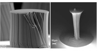
The process involves immersing vertically grown carbon nanotube bundles into a liquid organic solvent and allowing them to dry, which will cause the nanotubes to pull close together into a dense bundle, with a 25-fold increase in density.
"It's a significant and critical step toward the realization of carbon nanotube interconnects with better performance than copper," Lu said of his research findings. "But there's still a lot of work to do before this technology can be integrated into industrial applications."
The image is striking, as the same nanotube bundle looks like a "before" and "after" picture in a commercial for a diet, and the result is a bundle that looks more like a nail that like the folded rug it previously resembled.

 14 DAY TRIAL //