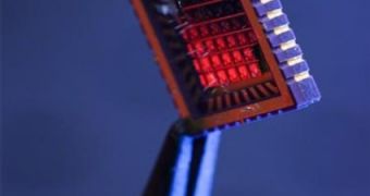
The device used in order to generate the pure spin current, produced at the Naval Research Laboratory, modulates and electrically detects pure spin in silicon semiconductors, mostly used in electronic devices. A silicon n-type layer enables the generation of a spin current, with the help of magnetic contacts placed on its surface, which circulate separately from the electrically charge current generated. The voltage of the spin orientation is detected in the second magnetic contact. The spin orientation is controlled in the silicon channel, by the help of the relative magnetization of the contacts, in a lateral transport geometry through lithographic techniques.
The demonstration of the first device that generates a pure spin current represents a key step in the technology which develops devices, also known as 'semiconductor spintronics'; these are expected to lead to new electronic devices that use spin currents instead of electrical currents, with high performance and lower power consumption.
Though technology has made big steps in developing even smaller electronic devices, and has continuously improved their performance, the size scaling does not present a viable solution to developing better devices. Thus, scientists turned towards using the quantum properties of matter, such as the spin angular momentum of the electron that can be used to store and process information in certain materials, like metals or semiconductors.
Originally discovered in 1988, the magnetorsistance phenomenon, originating from the spin-polarized electron currents inside metals, has been used in order to create a wide variety of commercial products, such as high density computer hard drives. Also, the physicist who discovered the effect has been awarded this year's Nobel Prize for Physics.
However, while the spin angular momentum can only be used for applications to store and process information, it can be used in metals, exclusively. As a result, the International Technology Roadmap for Semiconductors has decided to explore the possibility of replacing the electrons charge from electronic devices with the electrons spin. Nevertheless, until the success of the experiment made at NRL, the control of a pure spin current was somehow more fiction than fact.
The original experiments made by NRL in this field were made mostly on III-V semiconductors, which had direct band gaps of gallium arsenide that gave powerful insight of the behavior of the spin system, as these powerful optical spectroscopy techniques are relatively easy to apply. Important advances have been made recently, by using spin transport in semiconductors without a direct gap material, which proves to be an efficient injection of spin-polarized electrons with the help of ferromagnetic metal contacts.
However, this is only very recent work, generating pure spin currents flowing in opposite direction and producing spin current shifts in the electrochemical potential that can be detected in a second magnetic contact as voltage.
The relative orientation of the spin in the semiconductor material and the magnetization of the contact are closely related to the amount of voltage applied to the structure, and the spin can be uniformly rotated with the help of a magnetic field, through a process known as coherent precession.

 14 DAY TRIAL //