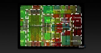
Although the official announcement came about two months back, details about Nvidia's upcoming Project Denver CPUs have been scarce until now, but this is no longer the case as the first die-shot of such a core has already been released, giving us a sneak peak inside this 64-bit ARM-based processor.
The image was revealed during a presentation held by Jen-Hsun Huang, Nvidia's chief executive officer and president, during the 2011 Financial Analyst Day.
As expected, no information regarding the size, or the manufacturing process, of the core were disclosed, since this is still based on early silicon and all these are subject to change.
What seems surprising, when taking a look at Nvidia's diagram, is the amount of die space occupied by the L1 data cache, which seems to suggests that the CPU will feature a massive amount of L1 cache, probably larger than the L2 cache size.
According to Bright Side of News, Nvidia said during the presentation that four Project Denver cores can be attached to a high-bandwidth interface such as existing GPU memory controller.
Since Project Denver is expected to launch at about the same time as Nvidia's Maxwell GPU architecture this would mean that the CPU could have access to more than 2TB/s of internal bandwidth and 320GB/s of external memory bandwidth if embedded inside this graphics core.
This would clearly exceed even the fastest processors available right now, but would also limit the amount of memory that the cores can access as graphics cards usually have limited amounts of video buffer available, when compared to a x86 system.
Project Denver is designed to support future products ranging from personal computers and servers to workstations and supercomputers.
According to previous reports, the CPU is based on a 64-bit ARM processor architecture and Nvidia says it has been in development for about three and half years.

 14 DAY TRIAL //