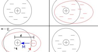
The “dielectric confinement effect,” first proposed in 1979 by scientist L. V. Keldysh, has finally been confirmed with measurements conducted by a team of researchers from the Harvard School of Engineering and Applied Sciences (SEAS), working together with colleagues from the Worcester Polytechnic Institute (WPI). They have shown that the activation energy of impurities in semiconductor nanowires is directly related to the surrounding dielectric. In addition, the investigators have also proven that, by changing the nanowire-embedding medium, the activation energy can be modified according to the needs of the experiment in which the material is used.
Modifying these features can lead to a change in the conductivity properties of the entire material, which can significantly benefit the design, development and construction stages of new electronic devices, such as gas or liquid substance detectors. “The demonstrated effect sets in as circuit dimensions shrink, which makes the material more sensitive to external conditions,” SEAS John A. and Elizabeth S. Armstrong Professor of Physics Venkatesh Narayanamurti, who is also the lead author of a new study detailing the finds, argues.
The paper, which was published today, in the April 6th issue of the scientific journal Applied Physics Letters, also opens up new avenues of research in improving the performances and overall design of nanowire electronic and optoelectronic devices. Also part of the research have been SEAS graduate student Joonah Yoon, the co-author of the study, and WPI graduate student Alexi Girgis.
Basically, what the researchers did was to discover a way of influencing the charge that the nanowires had, from the outside. That is to say, the surface of this class of materials acts like a mirror for the charge within, but, when the mirror is far, the influence that it has on the charge is close to none. However, on a nanoscale, when the mirror surface is extremely close to the device itself, the influence grows significantly, making it possible to manipulate the charge inside the nanowire by directly applying modifications to the mirror.
“Our key finding was that devices made with nanowires, such as nanowire field-effect transistors, require imaginative design of the materials, the surrounding dielectric, and the operating voltage bias to take into account dielectric confinement effects,” Narayanamurti concluded.

 14 DAY TRIAL //