The need of improvement has something to do with our attempt to evolve, but instead of learning manners and how to behave as individuals in a society, we try to better the things around us while we grow more and more dependant of the technology. In Ancient Greece, there was a greater deal of manual labor, almost all of the things one person did were closely related to having to move stuff around. Therefore, in the sculptures the Greeks were depicted as being super-built humans with muscles of steel, and this, in turn, gave room for a lot of stories that we should more often tell our children in the evening.
Nowadays, we tend to do just the opposite, taking the manual labor away from us and letting the machines do the work instead. The behavior is influenced by the technology that surrounds us, children are born with computers in their lap, the Internet is becoming increasingly available to more and more homes and the worst part of it is that we also let the machines do the thinking for us. That translates into poor education, lack of skill, no immediate need of a knowledge base, people tend to "wing it", "play it by the ear" and so on.
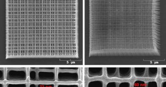
And in this need of being cozier, our lazy selves strive to create technologies that would help this trend evolve even more. One of the domains in which a continuous effort is put into developing increasingly small manufacturing technologies is the processor industry. And even though it isn't a new process node that's being developed, the researchers at the Georgia Institute of Technology and Focal Point Microsystems have devised a way of manufacturing a cheaper pattern for the 65nm process node. The process is called 3D multiphon lithography, by coating the wafers with a special polymer called DAPB (di-n-butylaminobiphenyl) and then shaping them with a laser, all that remains is to etch off the remaining polymer and a nanoscale 3D structure is what comes out of the process.
Georgia Tech professor Joseph Perry said: "With our technique, we can use polymers to define features on silicon in a manner similar to traditional approaches, but our method provides a much lower-cost way of making such nanoscale patterns. The laser cross-links the polymer, which is a process of making bonds between polymer chains that leads to the formation of a highly interconnected network of polymer. This process renders the cross-linked material insoluble. We already have efficient materials that should allow for fabrication at high speeds. Our biggest technical hurdle now is instrumentation: We need faster instruments to increase the throughput of the fabrication process."

 14 DAY TRIAL //