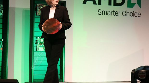
Chip manufacturer Advanced Micro Devices has introduced its 45-nanometer Opteron chips with Shanghai core and the 45 Phenoms in the Deneb core family at yesterday's public conference. The company is still far from releasing the chips for mass-availability, yet this is a proof that AMD is still in track with the 2008 release.
The AMD officials refused to detail upon any of the chip's technical specifications, such as clock speeds and power consumption. The first generation of 45-nanometer chips will be produced using AMD's immersion lithography process, but AMD is currently working with IBM at perfecting the EUV lithography technology. AMD has taken a different approach at the 45-nanometer technology than its Intel rival, as the chip manufacturer won't use high-k dielectric metal gate at this time.
According to the company, AMD's chips will be as competitive as Intel's offering without using hi-k gate at this time. However, AMD spokesperson Gary Silcott claimed that high-k will be an option that will probably be introduced in the next step of the 45-nanometer technology, and "definitely at the 32-nanometer".
AMD seems to gear up for a slight delay of its 45-nanometer products. In June 2006, AMD's chief operating officer Dirk Meyer had said that the company would get closer to Intel in terms of technology as far as the x86 business is concerned. Back then, he told chip analysts that the company would release its 45-nanometer units 18 months after the introduction of its 65-nanometer products. The same timeline estimated that the company would have ramped up production of its 45-nanometer chips by June 2008. This means that Intel will not have a full year advantage over AMD, but rather 6 months.
The company had announced last October that it started sampling production of its 45-nanometer processors, yet the first SRAM silicon had been shown a little earlier, in May.

 14 DAY TRIAL //
