 14 DAY TRIAL //
 Carbon nanotubes, though a relatively recent find, have fueled the imagination of many scientists, who strongly believe that they are the future of electronic circuitry and so, the successors of silicon, who by now has almost reached the limit of its applications.
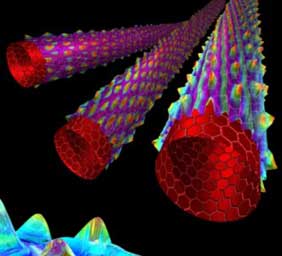
They are allotropes (two or more crystalline or molecular structural forms of the same element) of carbon. A carbon nanotube is a one-atom thick sheet of graphite (called graphene) rolled up into a seamless cylinder with diameter of the order of a nanometer. This results in a nanostructure where the length-to-diameter ratio exceeds 10,000. Such cylindrical carbon molecules have novel properties that make them potentially useful in a wide variety of applications in nanotechnology, electronics, optics and other fields of materials science. They exhibit extraordinary strength and unique electrical properties, and are efficient conductors of heat. Inorganic nanotubes have also been synthesized.
Nanotubes made of a single layer of carbon atoms can be regarded as individual sheets (one atom thick) of graphite which are wrapped up to form tubes. It is the diameter of the tube and the degree of helicity (the component of the spin of a particle along its momentum) in this wrapping which determine the electronic properties. Different configurations can result in the tube behaving either as a metallic conductor or as a semiconductor, and this theoretically-predicted relationship between the structure and electronic properties has been confirmed using scanning tunnelling microscopy.
Now, researchers at the University of Surrey have shown for the first time that knowing the structure of the surface layer of a multi-layer carbon nanotube is not enough to predict its electronic properties.
These new experiments used scanning tunnelling microscopy of double-walled carbon nanotubes to demonstrate an explicit correlation between the helicity of the constituent tubes, their electronic coupling and the overall electronic structure.
Cristina Giusca, the lead author of the paper said: "The work is of fundamental importance to the carbon community as it shows the first evidence for a direct correlation between the electronic properties of multiwall carbon nanotubes and the diameter and chiral indices (helicity) of the inner shells".
Professor Ravi Silva, who leads the Advanced Technology Institute at the University of Surrey, indicated that "This is a fine example of the cutting edge research undertaken at the Institute which combines the very best in fundamental research with sound theoretical backing. The work is of crucial importance to all of us conducting research in carbon nanotubes and other forms of quantum transport studies in 1D structures which clearly highlights the importance of the electronic interaction between adjacent layers, which were previously considered to be less important. This work will add new vigor to those examining the use of carbon nanotubes for interconnects in the IC industry. Having only metallic carbon nanotubes may now not be necessary in the design of interconnect wires between semiconductors if multi-walled nanotubes are to be used for this application."
The new finds are a major step in understanding the processes of nanotubes manufacturing, and thus a wider application area, since single and multi-walled nanotubes can produce materials with toughness un-matched in the man-made and natural world.