Softpedia
 

NEWS CATEGORIES:


NEWS ARCHIVE >>
SOFTPEDIA REVIEWS >>
MEET THE EDITORS >>
Home > News > Editor Blogs > Technology

January 5th, 2012, 11:05 GMT · By

BLOG

Asus Transformer Prime Gets Teardown Treatment

SHARE:

Adjust text size:

Asus Transformer Prime teardown Enlarge picture - Asus Transformer Prime teardown
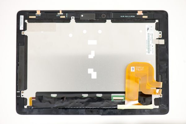
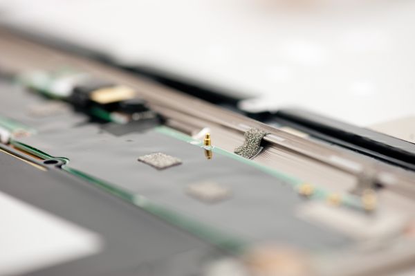
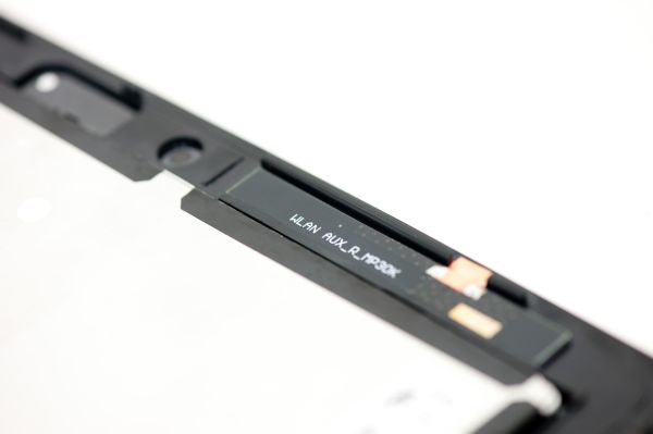
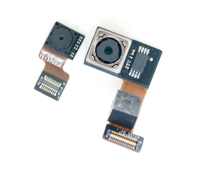
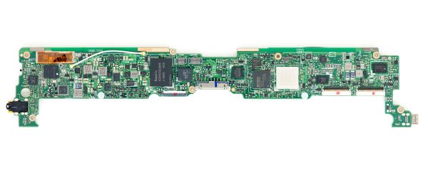
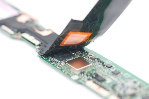
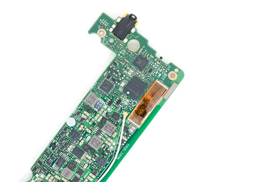
If you ever wondered what’s inside Asus’ Transformer Prime now is your chance to find out as the tablet was the subject of a detailed image teardown.

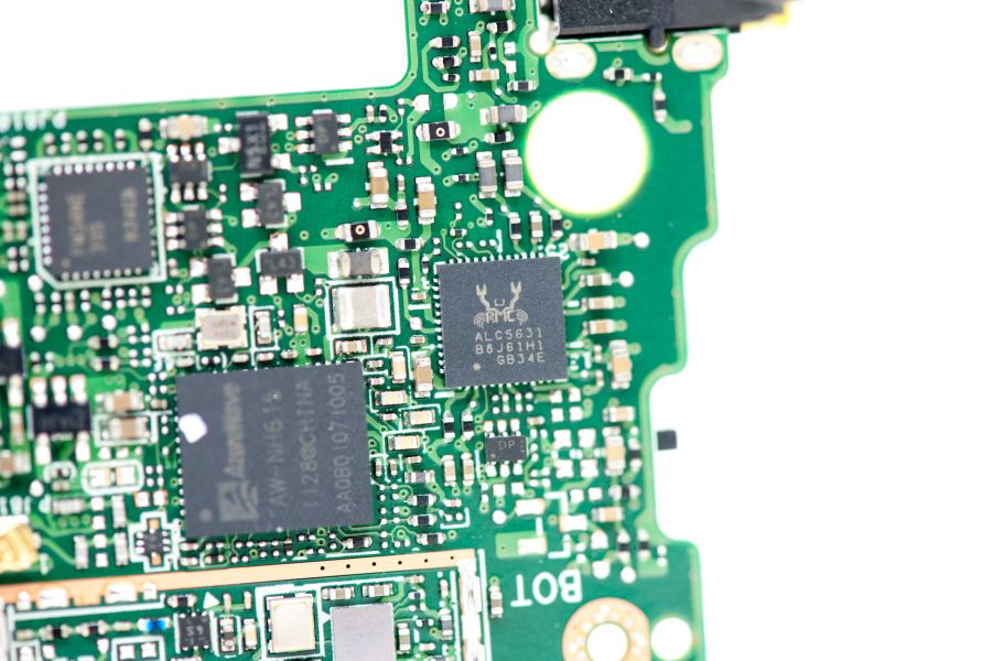
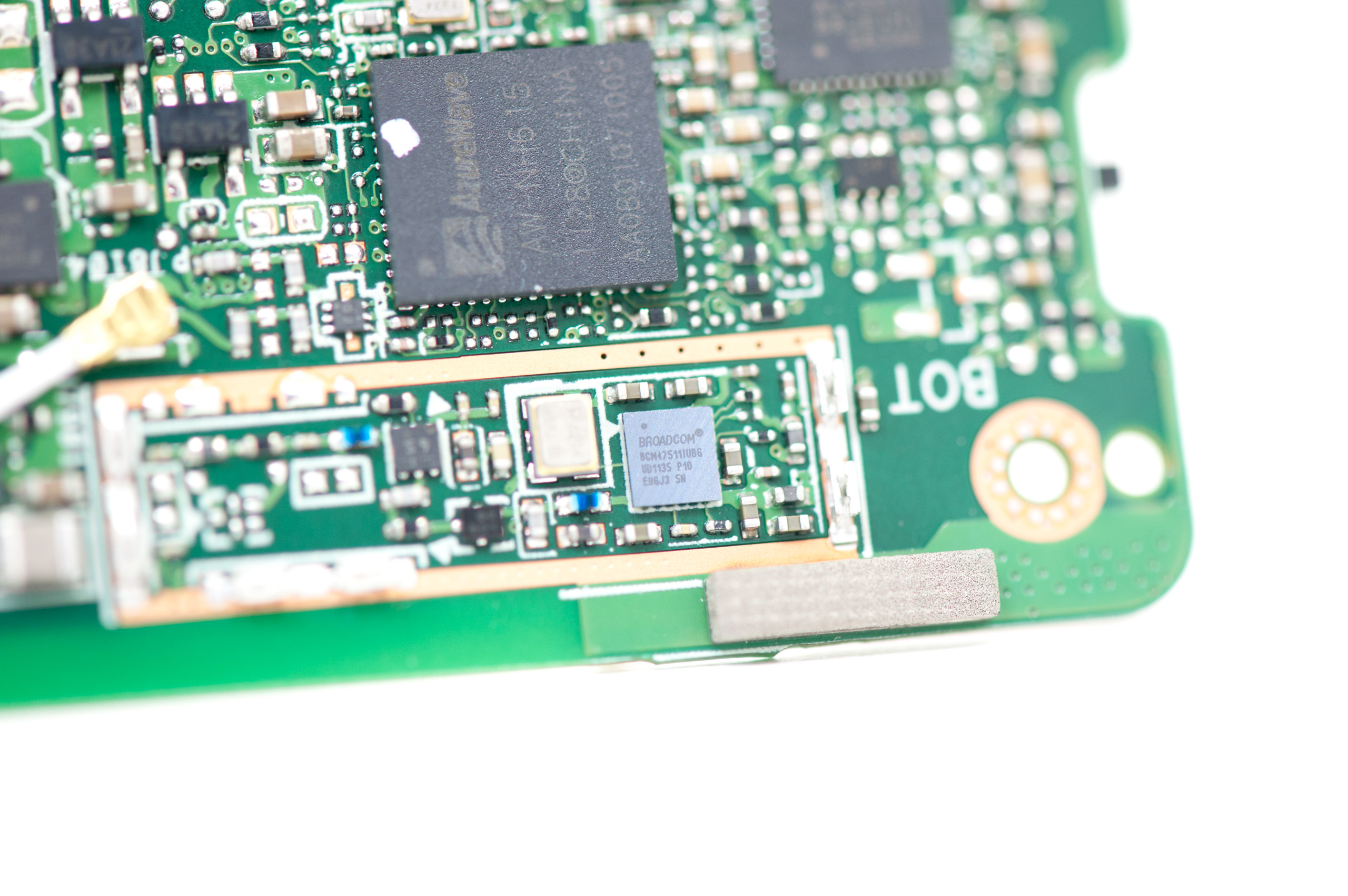
Published by AnandTech, the teardown goes to great length to show us the insides of the Prime, including the tablet’s quad-core Nvidia Tegra 3 SoC.

Of course that this isn’t the only thing that one would find inside the Transformer Prime as the chip is also accompanied by 32GB of Hynix e-NAND memory (basically a single chip SSD), 1GB of Elpida LPDDR2 DRAM an Azurewave WiFi controller as well as other bits and pieces.

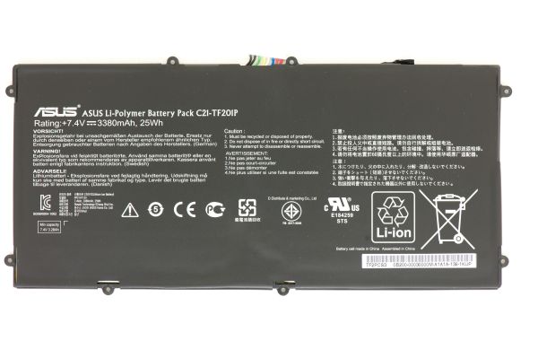
The Broadcom BCM4751 GPS receiver and that troublesome GPS antenna are also packed in there, together with a large battery that takes out most of the available space.

For more pictures and detailed tear down instructions for the Transformer Prime head on over to the AnandTech website.


ASUS TRANSFORMER PRIME TEARDOWN - PHOTO GALLERY:

TELL US WHAT YOU THINK:

2,931 hits · Link to this article · Print article · Send to friend · Subscribe to news

MUST-READ RELATED ARTICLES:


Asus Transformer Prime GPS Issues Explained

Asus Transformer Prime Android 4.0 ICS Update Due January 12

Asus Responds to Transformer Prime’s Locked Bootloader, Battery & GPS Issues

Sony Cuts Tablet S Price by $100 (€76.8), Now Starts at $399 (€306)

Toshiba’s Upcoming Nvidia Tegra 3 Tablet Presumably Spotted

READER COMMENTS:


No user comments yet.
Be the first to express your opinion!
Copyright © 2001-2012 Softpedia. Contact/Tip us at

WindowsGamesDriversMacLinuxScriptsMobileHandheldNews

SUBMIT PROGRAM   |   ADVERTISE   |   GET HELP   |   SEND US FEEDBACK   |   RSS FEEDS   |   UPDATE YOUR SOFTWARE   |   ROMANIAN FORUM