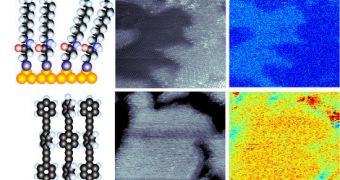
Investigators have developed a new set of tools for studying various phenomena taking place at the nanoscale, which is extremely important for innovating today's electronics.
For years, physicists have been working on decreasing the size of various components that form the basis of electronic devices, and, as they did so, they ran into various problems. One of them is that the interactions taking place between materials at the nanoscale is still a mystery.
As such, the need was great for developing a method of analyzing them in great details. Scientists have recently responded to that need, by developing a dual scanning tunneling and microwave-frequency probe, which experts say could revolutionize the field.
The device was produced by experts at the University of California in Los Angeles (UCLA), who were led by the Fred Kavli Chair in NanoSystems Sciences, Paul Weiss.
The instrument itself is capable of analyzing interactions that develop between single molecules and the surfaces on which scientists want to attach the molecules to. Using the new technique, scientists may become able to exploit the phenomena they discover to their own advantage.
“Our probe can generate data on the physical, chemical, and electronic interactions between single molecules and substrates, the contacts to which they are attached,” Weiss explains.
“Just as in semiconductor devices, contacts are critical here,” adds the expert, who also holds an appointment as the director of the California NanoSystems Institute at UCLA. He is a distinguished professor of chemistry and biochemistry & materials science and engineering at the university.
Northwestern University theoretical chemist Mark Ratner and Rice Universitysynthetic chemist James Tour were also a part of the team that conducted the experiments. Details of the work appear in the latest issue of the scientific journal ACS Nano.
In the journal entry, the team details a probe capable of simultaneous scanning tunneling microscopy (STM) measurements and microwave difference frequency (MDF) measurements, and provide details of possible applications in store for it.
One of the most remarkable things about the probe itself is that it can be used to conduct a wide variety of measurements. It is equally as useful for conducting physical, chemical and electronic studies.
As such, investigators could use them to search for and identify structures at the sub-molecular level, inside complex biomolecules and assemblies, among other nanoscale structures.

 14 DAY TRIAL //