14 DAY TRIAL //
 A couple of days ago, we reported that AMD is preparing to launch a triple-core version of its Llano accelerated processing units, and today, after a bit of digging around, we managed to find the first pictures of this APU as well as a series of screenshots, which confirm its specifications.
All the information was uncovered on a Chinese forum, which also provided a series of benchmark results to indicate the performance of the chip.
AMD's new APU will be called the A6-3500 and its specifications closely resemble those of the A6-3600, except for the fourth computing core that was disabled by AMD.
This means that the chip has a base frequency of 2.1GHz, which can go up to 2.4GHz thanks to AMD's Turbo Core technology, 3MB of Level 2 cache memory, and an integrated Radeon HD 6530D GPU.
The second slowest integrated graphics core in the Llano lineup, the HD 6530D includes 320 stream processors clocked at 433MHz, and is compatible with the company's Hybrid CrossFireX technology for enabling dual-graphics operation.
Outside of the on-die graphics core, the new Llano APU will also feature an integrated dual-channel DDR3-1866MHz memory controller and a 16-lane PCI Express Gen 2.0 controller, while its TDP is rated at the same 65W as that of the A6-3600.
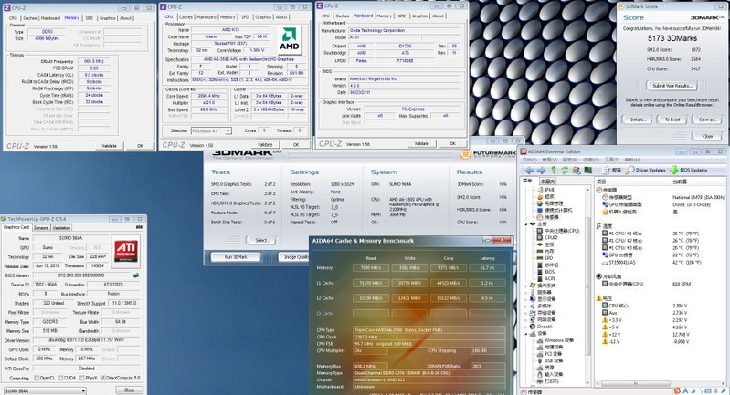
In order to test the performance of the tri-core Llano chip, the user run both 3DMark 06 and the cache & memory benchmark from the AIDA64 software suite. In the first of the two scenarios, the A6-3500 managed to achieve a score of 5173 3D marks.
Sadly, the user hasn't tried to unlock the fourth disabled core, so we don't know if this chip can be turned into a cheap quad-core part.
The new AMD A6-3500 triple-core APU is expected to arrive in the third quarter of this year at a yet-undisclosed price point.