14 DAY TRIAL //
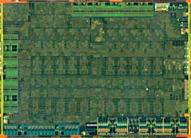
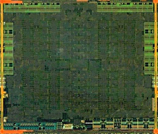
 The famous fabless CPU and GPU designer, American company Advanced Micro Devices has succeeded in launching the powerful GCN graphics architecture more than half a year ahead of its main competitor in this field.
AMD was not keen on showing Nvidia how it’s done so, at first, the traditional microchip semiconductor die shots were not available and what was released during the past months were very low-quality pictures.
The Texan company has reportedly decided that the time has come to show off the Southern Islands family in “full monty.”
Check out the gallery below to see how each 3D and GPU computing powerhouse looks on the inside.
The head picture depicts the full 4.3 billion transistors inside AMD famous Tahiti GPU built in TSMC’s 28nm manufacturing technology.