14 DAY TRIAL //
 We'd already known that AMD's new high-end graphics cards, Radeon R9 290/290X, would be based on a new CPU, but we didn't have a clear view of the chip itself, until now anyway.
The diagram of the upcoming Hawaii graphics processing unit has been leaked to the Internet, thanks to 3DCenter.org website.
This slide, or set of slides, popped up briefly on other websites too, but it was taken down due to NDAs. Apparently, the folks at 3DCenter decided to jump the gun anyway.
It's not all bad really. Not with the Radeon R9 290 and 290X graphics cards expected to make their appearance in a day or so.
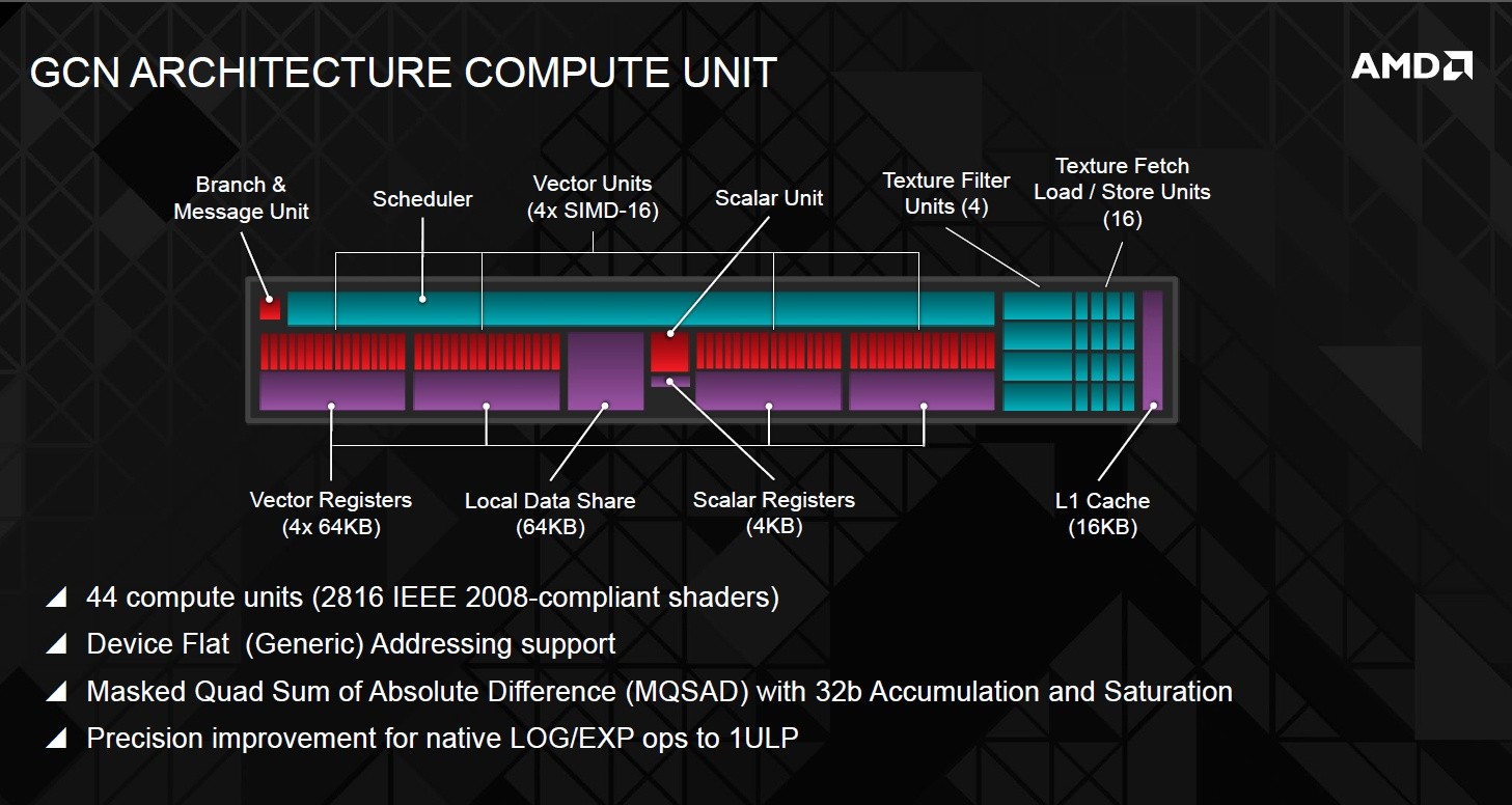
The Hawaii GPU has the same component hierarchy as Tahiti, but there is a very clear difference, in that Hawaii has four shader engines instead of just two.
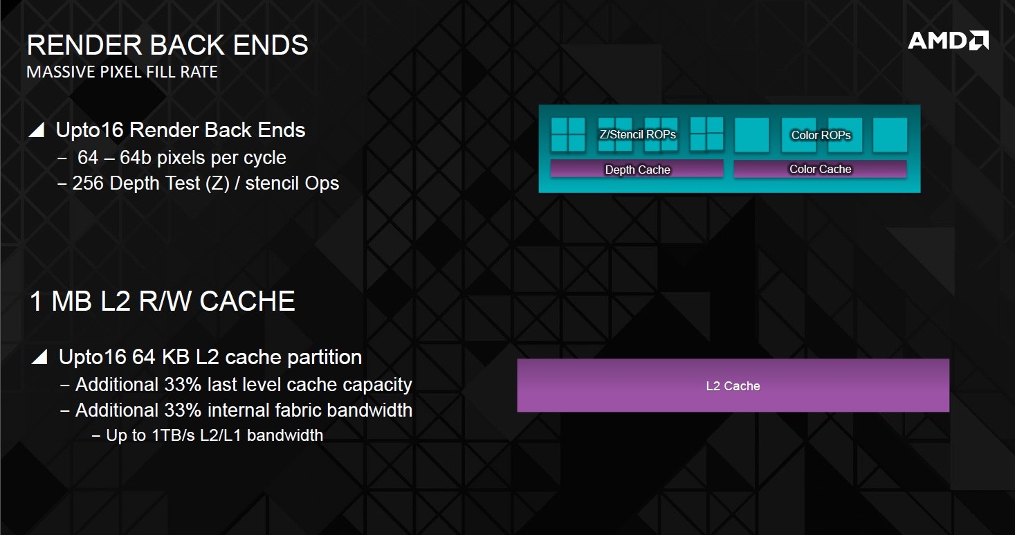
That means that Hawaii has twice the geometric processing power (four independent geometry processors with a tessellation unit each) and twice the number of ROPs (64).
Each of the four shader engines has 11 compute units too, responsible for parallel processing, while the 176 TMUs (texture memory units) are distributed among said CUs, the same way the 2,816 Stream Processors are grouped 64 per CU.
It is clear that Advanced Micro Devices really pulled out all the stops. Even if it couldn't move from the 28nm manufacturing technology, it refined its design enough to challenge NVIDIA's GeForce GTX Titan, despite its (presumably) lower price.
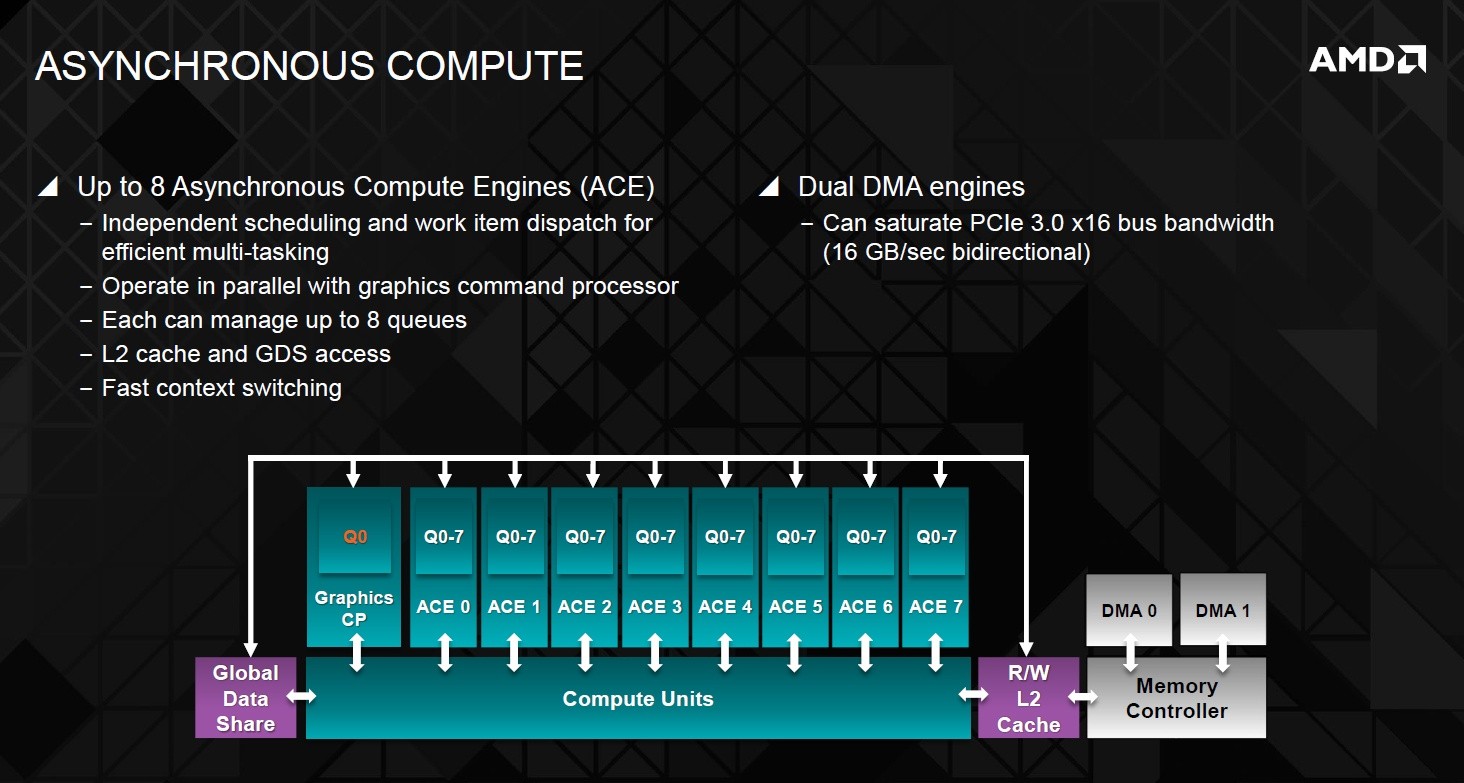
All four shader engines are tied together by a unified command processing structure and rely on 1 MB of L2 cache memory for quick data exchange and processing.
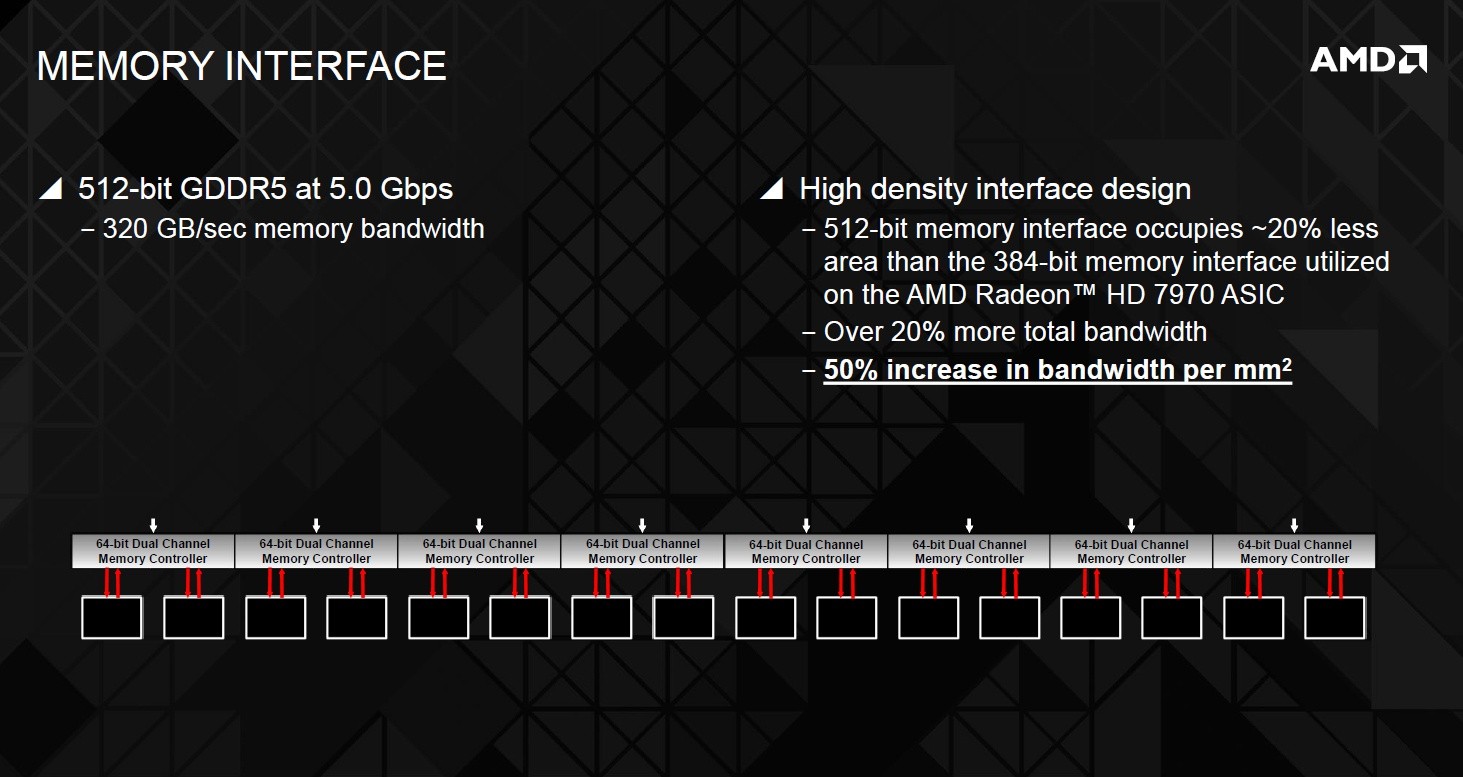
Finally, AMD's Hawaii GPU has a 512-bit wide GDDR5 memory interface, a PCI-Express 3.0 x16 bus interface, six display controllers, multimedia accelerators (UVD for HD video acceleration, CVE video codec engine, TrueAudio hardware sound technology) and CrossFireX XDMA.