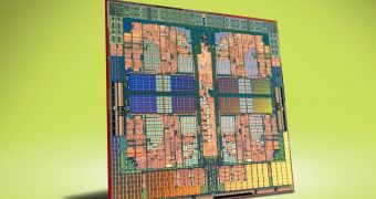
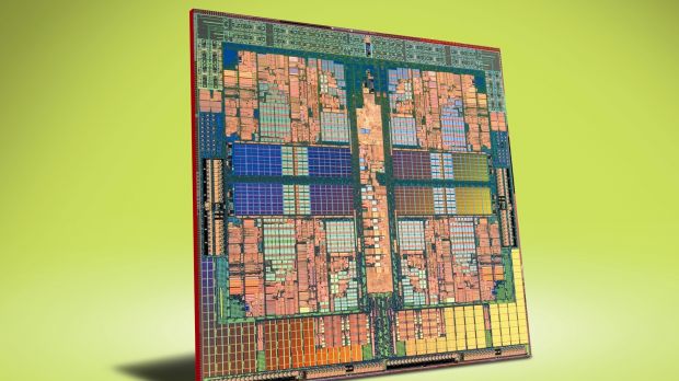
Manually designing some of the functional units on a microprocessor was possible and was a method often used back when a CPU had 100,000, a million, or tens of millions of transistors.
Before going ahead, you should read Part 1 of our AMD Hot Chips report.
Now that CPUs are going well beyond the 2-billion transistors mark, moving millions of transistors around on the design is a very complex operation that usually leads to a great increase in die size.
Also, hand drawing the layout is a very complex operation that can be heavily optimized by specialized software.
When transistor count is the criteria, the most popular complex chips are the GPUs that have reached and surpassed the 4-billion transistors mark back in 2011 with AMD’s Tahiti design.
Since Nvidia and AMD’s GPUs are made at TSMC and both designers pay the foundry for each processed silicon wafer, it is very important that they make as many GPUs per wafer as possible.
For this, each foundry usually provides its customers with automated microchip design tools that will take a design and rearrange the units and the transistors in a manner that’s best suited for that specific manufacturing technology.
This way, the specialized software makes the chips much smaller and also makes sure that everything works fine.
The design software usually goes for two things: the tightest and making sure everything works properly in the new, rearranged die plan.
When making networking or DPS processors, this is probably the best approach to get as much CPU dies per wafer and, therefore, the lowest manufacturing costs per chip.
One thing that might not appeal to enthusiasts is that these chips work at much lower frequencies than the ones with manual intervention on the die design.
Basically AMD’s Bulldozer might not easily reach 2 GHz, if its die design would be so crammed.
At 2 GHz, the internal units would likely work fine, but raising the frequency any higher would make the “hot” units give out errors or leak electrons that would affect the surrounding transistors.
Read about how the company is going to use such a design method on its CPUs in Part 3 of our AMD report, coming later this week. AMD Experiments with Different CPU Design Methods – Part 3.

 14 DAY TRIAL //
