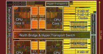
The upcoming 45-nanometer processors from AMD, called the Shanghai, have been showcased by the chip manufacturer back at the CeBIT. The 45-nanometer Shangai chips seem to feature the same die size as the rival products from AMD, the Nehalems. Of course, the discrepancy is minimal (243 square millimeters for the Shanghai, and 246 square millimeters for the Nehalem.
If the estimations released by Chip Architect's Hans de Vries are correct, AMD lacks the die size advantage previously touted by the company. However, other rumors claim that AMD is cooking a 0MiB version of the Shanghai/Deneb silicon, called Propus, that is targeted at the low-end market. It is alleged that the low-end version will feature a more than 30 percent smaller die size than the Nehalem chips.
According to Hans de Vries, the die size in the Shanghai chips is 243 square millimeters, or 263 square millimeters if we take the test logic into account. On the other side, Nehalem chips feature a die size of 246 square millimeters, or 265 square millimeters, test logic included. However, there might be an error in de Vries' estimations, given the fact that the Nehalem's die shot reveals a 192-bit version of the chip, especially tailored for hardcore computing, while the Shanghai is an average, 128-bit + PCI Express version.
Stripping the L2 cache, Nehalems feature a much larger die size than the Shanghai chips, namely 24.4 square millimeters as compared to 15.3 square millimeters, but this is understandable, because unlike the Shanghai chips, Nehalems offer hyperthreading capabilities for each of the chip's cores. Given the difference, it seems that the Shanghai chips won't be able to match the Nehalems' performance.
The upcoming Shanghai chips will be built using a new technology process called "immersion lithography", that allows AMD to create the layout of the chip in a single step rather than the conventional 2-step process. The new lithography technique is 40 percent more efficient than conventional lithography, and will result in cheaper 45-nanometer processors.

 14 DAY TRIAL //