 14 DAY TRIAL //
 Researchers at Purdue University are using a rare type of electron microscope to see how structures like carbon nanotubes form at the atomic level, information that will be crucial for nanotechnology to find practical applications in computing, electronics and other areas.
The new transmission electron microscope has been modified so that researchers can watch how atoms come together to form nanostructures as gases flow into a chamber in the presence of a metal catalyst. This is the same method used to make nanotubes in research labs and electronic devices in the semiconductor industry.
"Before we can consistently manufacture nanostructures that have the same specifications and qualities, we have to learn precisely how atoms interact and come together to form these structures," said Eric Stach, an associate professor of materials engineering who operates the microscope at the Birck Nanotechnology Center.
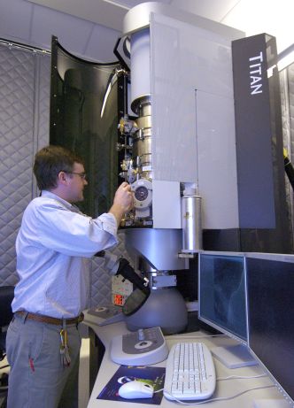
The $4 million FEI Titan microscope is equipped with an "environmental cell," in which gases such as acetylene or butane, which contain carbon, are passed over nanoparticles of metal, such as iron or nickel. The metal particles act as a catalyst for breaking down the gases and releasing carbon atoms during the reaction, which takes place in the cell at temperatures sometimes reaching more than 1,000 degrees Celsius (more than 1,800 degrees Fahrenheit).
"What's unusual about this instrument is the ability to take high-resolution pictures while you flow gases over a sample," said Stach, noting that fewer than five such microscopes exist in the world. The instrument, located in a new lab at Discovery Park, will allow researchers to take pictures of the internal structure of nanomaterials, capturing dynamic images of atomic motion during materials processing.
Electrons are accelerated under high voltage and manipulated with a series of "magnetic lenses" that focus electrons through thin sections of materials being studied. The electrons bounce off the atoms in the material, and this scattering process can be reconstructed to form an image.
"The transmission electron microscope allows you take pictures of the internal structure of a material," Stach said.
The instrument, which has 14 main lenses and another 50 smaller lenses, is housed in a specially shielded facility in the Discovery Park lab to block electromagnetic interference from sources such as powerlines and radio transmitters. The 3 meters-tall, 3 and a half-ton microscope sits on its own concrete slab, separated from the building's foundation to isolate it from vibration.
Pictures are formed with a resolution of 2 angstroms, which is fine enough to allow imaging of atomic arrangements in the sample.
"Researchers have done these sorts of experiments with other microscopes that have environmental cells but not with this level of resolution," Stach said.
Purdue researchers are using the microscope in a joint project with scientists at IBM Corp.'s Thomas J. Watson Research Center in Yorktown Heights, N.Y., to study how to make silicon nanowires for future computers.
For more information on the research conducted with this microscope see here (on carbon nanotubes) and here (on the creation of very small devices and structures from silicon and other semiconductor materials).
Photo: Eric Stach, an associate professor of materials engineering at Purdue University, loads a sample into the new FEI Titan electron microscope at the Birck Nanotechnology Center. Credit: Purdue News Service photo/ David Umberger