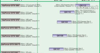
Leaks and rumors about what NVIDIA has in store have not been absent, but one has finally arisen that provides the exact plans of the company in regards to the 28nm manufacturing process.
28nm is the technology that both Advanced Micro Devices and NVIDIA rely on for their new series of graphics processing units (GPUs).
This report has now shown precisely how NVIDIA plans to have its Kepler advance.
The high-end chip will have a smaller die than the massive Fermi and will bear the name GK104.
With 384-bit memory support, it can churn out 2 TFLOPS (30% more than GTX 580) and will be ready by the middle of next year.
Unfortunately, the prowess comes at the price of a high power consumption, 250W, which makes one wonder how much energy the GK110, a dual GX104, will need (will appear soon after).
Much sooner than GK104 will arrive the GK107, the first model as it were, which is a notebook part, with a memory interface of 128 bits and PCI Express 2 support (other GK chips have PCI Express Generation 3 support).
The GK106 will come second, a mid-range GPU, featuring 256-bit memory. Along with the GX107, it will show up at some point during the second quarter of 2012.
So far, the Santa Clara company seems to have similar designs as AMD, but the similarities end at the end of 2012 / early 2013, when NVIDIA will again launch a GPU with a massive die: GX112, with 512-bit memory.
So far, things sound optimistic, but there is always a catch and, in this case, it is TSMC that might cause disruptions to this plan, as well as AMD's own.
Many fear that the nightmare behind the 40nm low chip yields, which hit both companies very hard last year, will repeat with 28nm.
The first signs are already showing in fact, as Taiwan Semiconductor Manufacturing Company is already experiencing a high demand while producing only 20,000 units per month.

 14 DAY TRIAL //